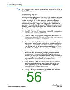
In System Programmability
would remain tri-stated if sampled) or to explicitly set a logic high, logic
low, or tri-state value on any pin. Setting these options is controlled on an
individual pin basis using the Quartus II software.
f
For more information, see the chapter on Real-Time ISP & ISP Clamp for
MAX II Devices.
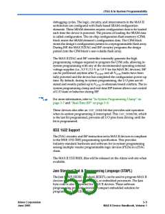
Real-Time ISP
For systems that require more than DC logic level control of I/O pins, the
real-time ISP feature allows you to update the CFM block with a new
design image while the current design continues to operate in the SRAM
logic array and I/O pins. A new programming file is updated into the
MAX II device without halting the original design’s operation, saving
down-time costs for remote or field upgrades. The updated CFM block
configures the new design into the SRAM upon the next power cycle. It is
also possible to execute an immediate configuration of the SRAM without
a power cycle by using a specific sequence of ISP commands. The
configuration of SRAM without a power cycle takes a specific amount of
time (tCONFIG). During this time, the I/O pins are tri-stated and weakly
pulled-up to VCCIO
.
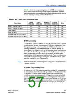
Design Security
All MAX II devices contain a programmable security bit that controls
access to the data programmed into the CFM block. When this bit is
programmed, design programming information, stored in the CFM
block, cannot be copied or retrieved. This feature provides a high level of
design security because programmed data within flash memory cells is
invisible. The security bit that controls this function, as well as all other
programmed data, is reset only when the device is erased. The SRAM is
also invisible and cannot be accessed regardless of the security bit setting.
The UFM block data is not protected by the security bit and is accessible
through JTAG or logic array connections.
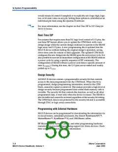
Programming with External Hardware
MAX II devices can be programmed by downloading the information via
®
in-circuit testers, embedded processors, the Altera ByteblasterMV™,
MasterBlaster™, ByteBlaster™ II, and USB-Blaster cables.
BP Microsystems, System General, and other programming hardware
manufacturers provide programming support for Altera devices. Check
their web sites for device support information.
3–8
Core Version a.b.c variable
Altera Corporation
June 2005
MAX II Device Handbook, Volume 1

 INTEL [ INTEL ]