Chapter 4. Hot Socketing &
Power-On Reset in MAX II
Devices
MII51004-1.4
MAX® II devices offer hot socketing, also known as hot plug-in or hot
swap, and power sequencing support. Designers can insert or remove a
MAX II board in a system during operation without undesirable effects to
the system bus. The hot socketing feature removes some of the difficulty
designers face when using components on printed circuit boards (PCBs)
that contain a mixture of 3.3-, 2.5-, 1.8-, and 1.5-V devices.
Hot Socketing
The MAX II device hot socketing feature provides:
■
■
■
Board or device insertion and removal
Support for any power-up sequence
Non-intrusive I/O buffers to system buses during hot insertion
MAX II Hot-Socketing Specifications
MAX II devices offer all three of the features required for hot socketing
capability listed above without any external components or special
design requirements. The following are hot-socketing specifications:
■
■
The device can be driven before and during power-up or power-
down without any damage to the device itself.
I/O pins remain tri-stated during power-up. The device does not
drive out before or during power-up, thereby affecting other buses in
operation.
■
Signal pins do not drive the VCCIO or VCCINT power supplies. External
input signals to device I/O pins do not power the device VCCIO or
VCCINT power supplies via internal paths. This is true for all device
I/O pins only if VCCINT is held at GND. This is true for a particular I/O
bank if the VCCIO supply for that bank is held at GND.
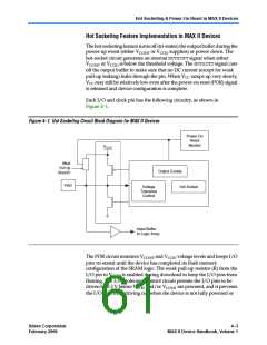
Devices Can Be Driven before Power-Up
Signals can be driven into the MAX II device I/O pins and GCLK[3..0]
pins before or during power-up or power-down without damaging the
device. MAX II devices support any power-up or power-down sequence
(VCCIO1, VCCIO2, VCCIO3, VCCIO4, VCCINT), simplifying system-level design.
Altera Corporation
February 2006
Core Version a.b.c variable
4–1
Preliminary

 INTEL [ INTEL ]