JTAG & In-System Programmability
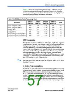
Table 3–4 shows the programming times for MAX II devices using in-
circuit testers to execute the algorithm vectors in hardware. Software-
based programming tools used with download cables are slightly slower
because of data processing and transfer limitations.
Table 3–4. MAX II Device Family Programming Times
EPM240
EPM240G
EPM570
EPM570G
EPM1270
EPM1270G EPM2210G
EPM2210
Description
Units
Erase + Program (1 MHz)
Erase + Program (10 MHz)
Verify (1 MHz)
1.72
1.65
0.09
0.01
1.81
1.66
2.16
1.99
0.17
0.02
2.33
2.01
2.90
2.58
0.30
0.03
3.20
2.61
3.92
3.40
0.49
0.05
4.41
3.45
sec
sec
sec
sec
sec
sec
Verify (10 MHz)
Complete Program Cycle (1 MHz)
Complete Program Cycle (10 MHz)
UFM Programming
The Quartus II software, with the use of POF, Jam, or JBC files, supports
programming of the user flash memory (UFM) block independent from
the logic array design pattern stored in the CFM block. This allows
updating or reading UFM contents through ISP without altering the
current logic array design, or vice versa. By default, these programming
files and methods will program both the entire flash memory contents,
which includes the CFM block and UFM contents. The stand-alone
embedded Jam STAPL player and Jam Byte-Code Player provides action
commands for programming or reading the entire flash memory (UFM
and CFM together) or each independently.
f
For more information, see the chapter on Using Jam STAPL for ISP via an
Embedded Processor.
In-System Programming Clamp
By default, the IEEE 1532 instruction used for entering ISP automatically
tri-states all I/O pins with weak pull-up resistors for the duration of the
ISP sequence. However, some systems may require certain pins on
MAX II devices to maintain a specific DC logic level during an in-field
update. For these systems, an optional in-system programming clamp
instruction exists in MAX II circuitry to control I/O behavior during the
ISP sequence. The in-system programming clamp instruction enables the
device to sample and sustain the value on an output pin (an input pin
Altera Corporation
June 2005
Core Version a.b.c variable
3–7
MAX II Device Handbook, Volume 1

 INTEL [ INTEL ]