Chapter 1: Cyclone IV Device Datasheet
1–9
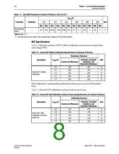
Operating Conditions
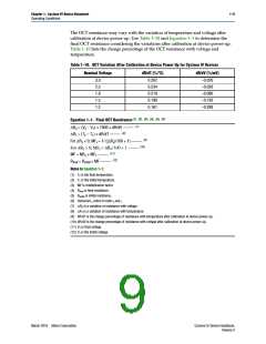
The OCT resistance may vary with the variation of temperature and voltage after
calibration at device power-up. Use Table 1–10 and Equation 1–1 to determine the
final OCT resistance considering the variations after calibration at device power-up.
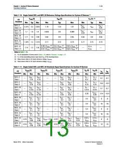
Table 1–10 lists the change percentage of the OCT resistance with voltage and
temperature.
Table 1–10. OCT Variation After Calibration at Device Power-Up for Cyclone IV Devices
Nominal Voltage
dR/dT (%/°C)
0.262
dR/dV (%/mV)
–0.026
3.0
2.5
1.8
1.5
1.2
0.234
–0.039
0.219
–0.086
0.199
–0.136
0.161
–0.288
Equation 1–1. Final OCT Resistance (1), (2), (3), (4), (5), (6)
(7)
RV = (V2 – V1) × 1000 × dR/dV –––––
(8)
RT = (T2 – T1) × dR/dT –––––
(9)
For Rx < 0; MFx = 1/ (|Rx|/100 + 1) –––––
(10)
For Rx > 0; MFx = Rx/100 + 1 –––––
(11)
MF = MFV × MFT –––––
(12)
Rfinal = Rinitial × MF –––––
Notes to Equation 1–1:
(1) T2 is the final temperature.
(2) T1 is the initial temperature.
(3) MF is multiplication factor.
(4) Rfinal is final resistance.
(5) Rinitial is initial resistance.
(6) Subscript x refers to both V and T.
(7) RV is a variation of resistance with voltage.
(8) RT is a variation of resistance with temperature.
(9) dR/dT is the change percentage of resistance with temperature after calibration at device power-up.
(10) dR/dV is the change percentage of resistance with voltage after calibration at device power-up.
(11) V2 is final voltage.
(12) V1 is the initial voltage.
March 2016 Altera Corporation
Cyclone IV Device Handbook,
Volume 3

 INTEL [ INTEL ]