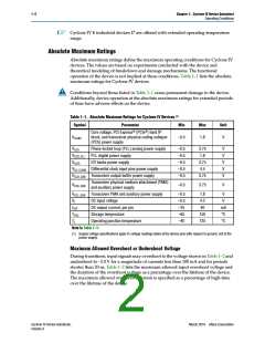
1–6
Chapter 1: Cyclone IV Device Datasheet
Operating Conditions
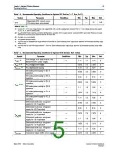
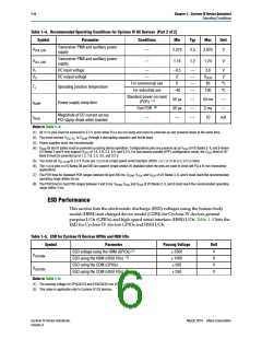
Table 1–4. Recommended Operating Conditions for Cyclone IV GX Devices (Part 2 of 2)
Symbol
VCCA_GXB
Parameter
Conditions
Min
Typ
Max
Unit
Transceiver PMA and auxiliary power
supply
—
2.375
2.5
2.625
V
Transceiver PMA and auxiliary power
supply
VCCL_GXB
—
1.16
1.2
1.24
V
VI
DC input voltage
DC output voltage
—
–0.5
0
—
—
—
—
3.6
VCCIO
85
V
V
VO
—
For commercial use
For industrial use
Standard power-on reset
0
°C
°C
TJ
Operating junction temperature
–40
100
50 µs
50 µs
—
—
—
—
50 ms
3 ms
10
—
—
(7)
(POR)
tRAMP
Power supply ramp time
(8)
Fast POR
Magnitude of DC current across
PCI-clamp diode when enabled
IDiode
—
mA
Notes to Table 1–4:
(1) All VCCA pins must be powered to 2.5 V (even when PLLs are not used) and must be powered up and powered down at the same time.
(2) You must connect VCCD_PLL to VCCINT through a decoupling capacitor and ferrite bead.
(3) Power supplies must rise monotonically.
(4) VCCIO for all I/O banks must be powered up during device operation. Configurations pins are powered up by VCCIO of I/O Banks 3, 8, and 9 where
I/O Banks 3 and 9 only support VCCIO of 1.5, 1.8, 2.5, 3.0, and 3.3 V. For fast passive parallel (FPP) configuration mode, the VCCIO level of I/O
Bank 8 must be powered up to 1.5, 1.8, 2.5, 3.0, and 3.3 V.
(5) You must set VCC_CLKIN to 2.5 V if you use CLKIN as a high-speed serial interface (HSSI) refclk or as a DIFFCLK input.
(6) The CLKIN pins in I/O Banks 3B and 8B can support single-ended I/O standard when the pins are used to clock left PLLs in non-transceiver
applications.
(7) The POR time for Standard POR ranges between 50 and 200 ms. VCCINT, VCCA, and VCCIO of I/O Banks 3, 8, and 9 must reach the recommended
operating range within 50 ms.
(8) The POR time for Fast POR ranges between 3 and 9 ms. VCCINT, VCCA, and VCCIO of I/O Banks 3, 8, and 9 must reach the recommended operating
range within 3 ms.
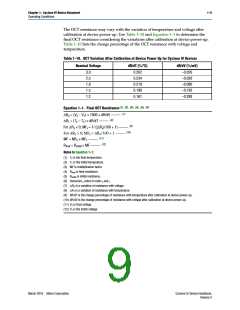
ESD Performance
This section lists the electrostatic discharge (ESD) voltages using the human body
model (HBM) and charged device model (CDM) for Cyclone IV devices general
purpose I/Os (GPIOs) and high-speed serial interface (HSSI) I/Os. Table 1–5 lists the
ESD for Cyclone IV devices GPIOs and HSSI I/Os.
Table 1–5. ESD for Cyclone IV Devices GPIOs and HSSI I/Os
Symbol
VESDHBM
Parameter
ESD voltage using the HBM (GPIOs) (1)
Passing Voltage
Unit
V
2000
1000
500
(2)
ESD using the HBM (HSSI I/Os)
V
ESD using the CDM (GPIOs)
V
VESDCDM
(2)
ESD using the CDM (HSSI I/Os)
250
V
Notes to Table 1–5:
(1) The passing voltage for EP4CGX15 and EP4CGX30 row I/Os is 1000V.
(2) This value is applicable only to Cyclone IV GX devices.
Cyclone IV Device Handbook,
Volume 3
March 2016 Altera Corporation

 INTEL [ INTEL ]