1–10
Chapter 1: Cyclone IV Device Datasheet
Operating Conditions
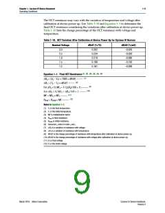
Example 1–1 shows how to calculate the change of 50-I/O impedance from 25°C at
3.0 V to 85°C at 3.15 V.
Example 1–1. Impedance Change
RV = (3.15 – 3) × 1000 × –0.026 = –3.83
RT = (85 – 25) × 0.262 = 15.72
Because RV is negative,
MFV = 1 / (3.83/100 + 1) = 0.963
Because RT is positive,
MFT = 15.72/100 + 1 = 1.157
MF = 0.963 × 1.157 = 1.114
R
final = 50 × 1.114 = 55.71
Pin Capacitance
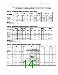
Table 1–11 lists the pin capacitance for Cyclone IV devices.
(1)
Table 1–11. Pin Capacitance for Cyclone IV Devices
Typical – Typical – Typical –
Quad Flat Quad Flat Ball-Grid
Symbol
Parameter
Unit
Pack
(QFP)
No Leads
(QFN)
Array
(BGA)
CIOTB
Input capacitance on top and bottom I/O pins
Input capacitance on right I/O pins
7
7
8
7
7
8
6
5
7
pF
pF
pF
CIOLR
CLVDSLR
Input capacitance on right I/O pins with dedicated LVDS output
CVREFLR
Input capacitance on right dual-purpose VREF pin when used as
21
21
23
21
23
pF
pF
(2)
VREF or user I/O pin
CVREFTB
Input capacitance on top and bottom dual-purpose VREF pin when
used as VREF or user I/O pin
(3)
23
(2)
CCLKTB
CCLKLR
Input capacitance on top and bottom dedicated clock input pins
Input capacitance on right dedicated clock input pins
7
6
7
6
6
5
pF
pF
Notes to Table 1–11:
(1) The pin capacitance applies to FBGA, UBGA, and MBGA packages.
(2) When you use the VREF pin as a regular input or output, you can expect a reduced performance of toggle rate and tCO because of higher pin
capacitance.
(3) CVREFTB for the EP4CE22 device is 30 pF.
Cyclone IV Device Handbook,
Volume 3
March 2016 Altera Corporation

 INTEL [ INTEL ]