Chapter 1: Cyclone IV Device Datasheet
1–5
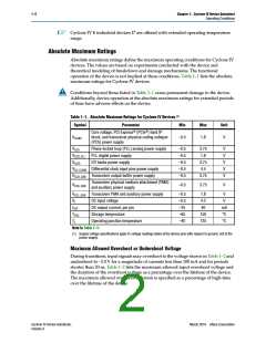
Operating Conditions
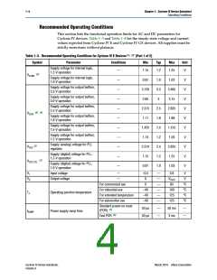
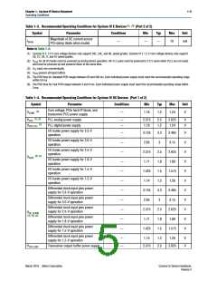
Table 1–3. Recommended Operating Conditions for Cyclone IV E Devices (1), (2) (Part 2 of 2)
Symbol
IDiode
Parameter
Conditions
Min
Typ
Max
Unit
mA
Magnitude of DC current across
PCI-clamp diode when enable
—
—
—
10
Notes to Table 1–3:
(1) Cyclone IV E 1.0 V core voltage devices only support C8L, C9L, and I8L speed grades. Cyclone IV E 1.2 V core voltage devices only support
C6, C7, C8, I7, and A7 speed grades.
(2) VCCIO for all I/O banks must be powered up during device operation. All VCCA pins must be powered to 2.5 V (even when PLLs are not used)
and must be powered up and powered down at the same time.
(3) VCC must rise monotonically.
(4) VCCIO powers all input buffers.
(5) The POR time for Standard POR ranges between 50 and 200 ms. Each individual power supply must reach the recommended operating range
within 50 ms.
(6) The POR time for Fast POR ranges between 3 and 9 ms. Each individual power supply must reach the recommended operating range within
3 ms.
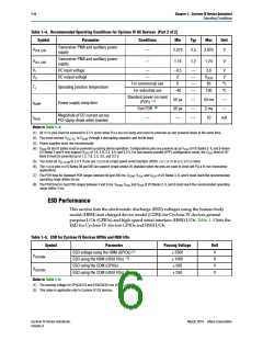
Table 1–4. Recommended Operating Conditions for Cyclone IV GX Devices (Part 1 of 2)
Symbol
Parameter
Conditions
Min
Typ
Max
Unit
Core voltage, PCIe hard IP block, and
transceiver PCS power supply
(3)
VCCINT
—
1.16
1.2
1.24
V
(1), (3)
VCCA
VCCD_PLL
PLL analog power supply
PLL digital power supply
—
—
2.375
1.16
2.5
1.2
2.625
1.24
V
V
(2)
I/O banks power supply for 3.3-V
operation
—
—
—
—
—
—
—
—
—
—
—
3.135
2.85
3.3
3
3.465
3.15
V
V
V
V
V
V
V
V
V
V
V
I/O banks power supply for 3.0-V
operation
I/O banks power supply for 2.5-V
operation
2.375
1.71
2.5
1.8
1.5
1.2
3.3
3
2.625
1.89
(3), (4)
VCCIO
I/O banks power supply for 1.8-V
operation
I/O banks power supply for 1.5-V
operation
1.425
1.14
1.575
1.26
I/O banks power supply for 1.2-V
operation
Differential clock input pins power
supply for 3.3-V operation
3.135
2.85
3.465
3.15
Differential clock input pins power
supply for 3.0-V operation
Differential clock input pins power
supply for 2.5-V operation
2.375
1.71
2.5
1.8
1.5
2.625
1.89
VCC_CLKIN
(3), (5), (6)
Differential clock input pins power
supply for 1.8-V operation
Differential clock input pins power
supply for 1.5-V operation
1.425
1.575
Differential clock input pins power
supply for 1.2-V operation
—
—
1.14
1.2
2.5
1.26
V
V
VCCH_GXB
Transceiver output buffer power supply
2.375
2.625
March 2016 Altera Corporation
Cyclone IV Device Handbook,
Volume 3

 INTEL [ INTEL ]