Chapter 1: Cyclone IV Device Datasheet
1–11
Operating Conditions
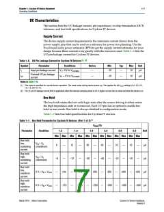
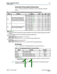
Internal Weak Pull-Up and Weak Pull-Down Resistor
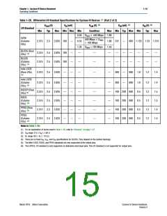
Table 1–12 lists the weak pull-up and pull-down resistor values for Cyclone IV
devices.
Table 1–12. Internal Weak Pull-Up and Weak Pull-Down Resistor Values for Cyclone IV Devices (1)
Symbol
Parameter
Conditions
Min
7
Typ
25
28
35
57
82
143
19
22
25
35
50
Max
41
Unit
(2), (3)
VCCIO = 3.3 V 5%
k
k
k
k
k
k
k
k
k
k
k
(2), (3)
(2), (3)
(2), (3)
(2), (3)
(2), (3)
(4)
V
CCIO = 3.0 V 5%
7
47
Value of the I/O pin pull-up resistor
before and during configuration, as
well as user mode if you enable the
programmable pull-up resistor option
VCCIO = 2.5 V 5%
8
61
R_PU
V
V
CCIO = 1.8 V 5%
CCIO = 1.5 V 5%
10
13
19
6
108
163
351
30
VCCIO = 1.2 V 5%
VCCIO = 3.3 V 5%
(4)
V
V
V
V
CCIO = 3.0 V 5%
CCIO = 2.5 V 5%
CCIO = 1.8 V 5%
CCIO = 1.5 V 5%
6
36
Value of the I/O pin pull-down resistor
before and during configuration
(4)
R_PD
6
43
(4)
7
71
(4)
8
112
Notes to Table 1–12:
(1) All I/O pins have an option to enable weak pull-up except the configuration, test, and JTAG pins. The weak pull-down feature is only available
for JTAG TCK
.
(2) Pin pull-up resistance values may be lower if an external source drives the pin higher than VCCIO
.
(3) R_PU = (VCCIO – VI)/IR_PU
Minimum condition: –40°C; VCCIO = VCC + 5%, VI = VCC + 5% – 50 mV;
Typical condition: 25°C; VCCIO = VCC, VI = 0 V;
Maximum condition: 100°C; VCCIO = VCC – 5%, VI = 0 V; in which VI refers to the input voltage at the I/O pin.
(4) R_PD = VI/IR_PD
Minimum condition: –40°C; VCCIO = VCC + 5%, VI = 50 mV;
Typical condition: 25°C; VCCIO = VCC, VI = VCC – 5%;
Maximum condition: 100°C; VCCIO = VCC – 5%, VI = VCC – 5%; in which VI refers to the input voltage at the I/O pin.
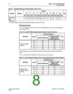
Hot-Socketing
Table 1–13 lists the hot-socketing specifications for Cyclone IV devices.
Table 1–13. Hot-Socketing Specifications for Cyclone IV Devices
Symbol
IIOPIN(DC)
Parameter
DC current per I/O pin
Maximum
300 A
(1)
IIOPIN(AC)
AC current per I/O pin
8 mA
IXCVRTX(DC)
DC current per transceiver TX pin
DC current per transceiver RX pin
100 mA
50 mA
IXCVRRX(DC)
Note to Table 1–13:
(1) The I/O ramp rate is 10 ns or more. For ramp rates faster than 10 ns, |IIOPIN| = C dv/dt, in which C is the I/O pin
capacitance and dv/dt is the slew rate.
1
During hot-socketing, the I/O pin capacitance is less than 15 pF and the clock pin
capacitance is less than 20 pF.
March 2016 Altera Corporation
Cyclone IV Device Handbook,
Volume 3

 INTEL [ INTEL ]