®
MOBILE PENTIUM PROCESSOR WITH MMX™ TECHNOLOGY
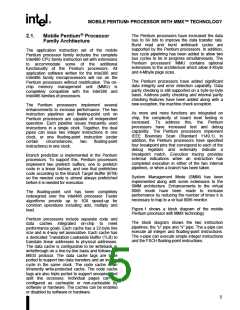
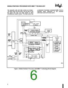
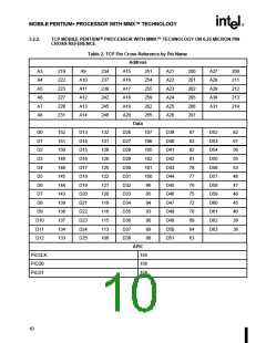
The separate code and data caches are shown,.
The data cache has two ports, one for each of the
two pipes (the tags are triple ported to allow
simultaneous inquire cycles). The data cache has
a dedicated Translation Lookaside Buffer (TLB) to
translate linear addresses to the physical
addresses used by the data cache.
Branch
Target
Buffer
Prefetch
Address
Code Cache
16 KBytes
128
nstruction
Pointer
I
Prefetch Buffers
Control
ROM
Instruction Decode
Branch Verif.
& Target Addr
64-Bit
Data
Bus
Control Unit
V-Pipeline
Connection
Floating-
Point
Unit
32-Bit
Address
Bus
U-Pipeline
Connection
Page
Unit
Bus
Unit
Control
Register File
Address
Address
Generate Generate
(U Pipeline) (V Pipeline)
TM
MMX
Unit
Control
Add
Integer Register File
Divide
80
ALU
ALU
(U Pipeline) (V Pipeline)
Barrel Shifter
64
Multiply
32
80
32-Bit
Addr.
Bus
64-Bit
Data
Bus
32
32
32
Data
Data Cache
32
32
16 KBytes
APIC
TLB
Control
32
PP011
Figure 1. Mobile Pentium ® Processor with MMX™ Technology Block Diagram
6

 INTEL [ INTEL ]