Electrical Specifications
3.3
3.4
Catastrophic Thermal Protection
The Celeron M processor supports the THERMTRIP# signal for catastrophic thermal
protection. An external thermal sensor should also be used to protect the processor
and the system against excessive temperatures. Even with the activation of
THERMTRIP#, which halts all processor internal clocks and activity, leakage current can
be high enough such that the processor cannot be protected in all conditions without
the removal of power to the processor. If the external thermal sensor detects a
catastrophic processor temperature of 125°C (maximum), or if the THERMTRIP# signal
is asserted, the VCC supply to the processor must be turned off within 500 ms to
prevent permanent silicon damage due to thermal runaway of the processor.
Signal Terminations and Unused Pins
All RSVD (RESERVED) pins must remain unconnected. Connection of these pins to VCC,
VSS, or to any other signal (including each other) can result in component malfunction
or incompatibility with future Celeron M processors. See Section 4.2 for a pin listing of
the processor and the location of all RSVD pins.
For reliable operation, always connect unused inputs or bidirectional signals to an
appropriate signal level. Unused active low AGTL+ inputs may be left as no connects if
AGTL+ termination is provided on the processor silicon. Unused active high inputs
should be connected through a resistor to ground (VSS). Unused outputs can be left
unconnected.
The TEST1 and TEST2 pins must have a stuffing option connection to VSS separately via
1-kΩ, pull-down resistors.
3.5
3.6
FSB Frequency Select Signals (BSEL[1:0])
The BSEL[1:0] signals are used to select the frequency of the processor input clock
(BCLK[1:0]). These signals should be connected to the clock chip and Intel 915PM/GM/
GMS and 910GML Express Chipset on the platform. These signals must be left
unconnected on platforms designed with the Celeron M processor and the Intel 852/
855 chipset families.
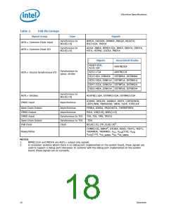
FSB Signal Groups
In order to simplify the following discussion, the FSB signals have been combined into
groups by buffer type. AGTL+ input signals have differential input buffers, which use
GTLREF as a reference level. In this document, the term “AGTL+ Input” refers to the
AGTL+ input group as well as the AGTL+ I/O group when receiving. Similarly, “AGTL+
Output” refers to the AGTL+ output group as well as the AGTL+ I/O group when
driving.
With the implementation of a source synchronous data bus comes the need to specify
two sets of timing parameters. One set is for common clock signals which are
dependant upon the rising edge of BCLK0 (ADS#, HIT#, HITM#, etc.) and the second
set is for the source synchronous signals which are relative to their respective strobe
lines (data and address) as well as the rising edge of BCLK0. Asychronous signals are
still present (A20M#, IGNNE#, etc.) and can become active at any time during the
clock cycle. Table 2 identifies which signals are common clock, source synchronous,
and asynchronous.
Datasheet
17

 INTEL [ INTEL ]