Electrical Specifications
3.7
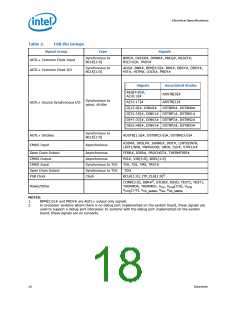
CMOS Signals
CMOS input signals are shown in Table 2. Legacy output FERR#, IERR# and other non-
AGTL+ signals (THERMTRIP# and PROCHOT#) utilize open drain output buffers. These
signals do not have setup or hold time specifications in relation to BCLK[1:0]. However,
all of the CMOS signals are required to be asserted for at least three BCLKs in order for
the processor to recognize them. See Section 3.9 for the CMOS signal group DC
specifications.
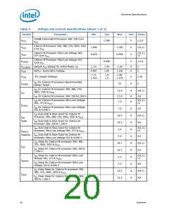
3.8
Maximum Ratings
Table 3 lists the processor’s maximum environmental stress ratings. The processor
should not receive a clock while subjected to these conditions. Functional operating
parameters are listed in the AC and DC tables. Extended exposure to the maximum
ratings may affect device reliability. Furthermore, although the processor contains
protective circuitry to resist damage from electro static discharge (ESD), one should
always take precautions to avoid high static voltages or electric fields.
Table 3.
Processor DC Absolute Maximum Ratings
Symbol
Parameter
Min
Max
Unit
Notes
TSTORAGE
VCC
Processor Storage Temperature
-40
-0.3
-0.1
-0.1
85
1.6
1.6
1.6
°C
V
2
Any Processor Supply Voltage with Respect to VSS
AGTL+ Buffer DC Input Voltage with Respect to VSS
CMOS Buffer DC Input Voltage with Respect to VSS
1
VinAGTL+
VinAsynch_CMOS
V
1, 2
1, 2
V
NOTES:
1.
2.
This rating applies to any processor pin.
Contact Intel for storage requirements in excess of one year.
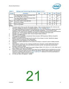
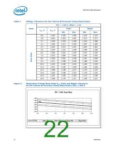
3.9
Processor DC Specifications
The processor DC specifications in this section are defined at the processor
core (pads) unless noted otherwise. See Table 2 for pin signal definitions and
signal pin assignments. Most of the signals on the FSB are in the AGTL+ signal group.
The DC specifications for these signals are listed in Table 9. DC specifications for the
CMOS group are listed in Table 10.
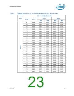
Table 4 through Table 10 list the DC specifications for the Celeron M processor and are
valid only while meeting specifications for junction temperature, clock frequency, and
input voltages. Active mode load line specifications apply in all states except in the
Deep Sleep state. VCC,BOOT is the default voltage driven by the voltage regulator at
power up in order to set the VID values. Unless specified otherwise, all specifications
for the Celeron M processor are at Tjunction = 100°C. Care should be taken to read all
notes associated with each parameter.
Datasheet
19

 INTEL [ INTEL ]