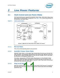
Low Power Features
is in the Sleep State, the SLP# and STPCLK# signals should be deasserted immediately
after RESET# is asserted to ensure the processor correctly executes the reset
sequence.
While in the Sleep state, the processor is capable of entering an even lower power
state, the Deep Sleep state by asserting the DPSLP# pin. (See Section 2.1.6.) While
the processor is in the Sleep state, the SLP# pin must be deasserted if another
asynchronous FSB event needs to occur.
2.1.6
Deep Sleep State
Deep Sleep state is a very low power state the processor can enter while maintaining
context. Deep Sleep state is entered by asserting the DPSLP# pin while in the Sleep
state. BCLK may be stopped during the Deep Sleep state for additional platform level
power savings. BCLK stop/restart timings on 855PM chipset family based platforms
with compatible clock generator chips are as follows:
• Deep Sleep entry - DPSLP# and CPU_STP# are asserted simultaneously. The clock
chip will stop/tristate BCLK within two BCLKs +/- a few nanoseconds.
• Deep Sleep exit - DPSLP# and CPU_STP# are deasserted simultaneously. The clock
chip will drive BCLK to differential DC levels within 2-3 ns and starts toggling BCLK
2-6 BCLK periods later.
To re-enter the Sleep state, the DPSLP# pin must be deasserted. BCLK can be restarted
after DPSLP# deassertion as described above. A period of 30 microseconds (to allow for
PLL stabilization) must occur before the processor can be considered to be in the Sleep
State. Once in the Sleep state, the SLP# pin must be deasserted to re-enter the Stop-
Grant state.
While in Deep Sleep state, the processor is incapable of responding to snoop
transactions or latching interrupt signals. No transitions of signals are allowed on the
FSB while the processor is in Deep Sleep state. Any transition on an input signal before
the processor has returned to Stop-Grant state will result in unpredictable behavior.
When the processor is in Deep Sleep state, it will not respond to interrupts or snoop
transactions.
2.2
FSB Low Power Enhancements
The Celeron M processor incorporates the FSB low power enhancements:
• Dynamic FSB Power Down
• BPRI# control for address and control input buffers
• Dynamic On Die Termination disabling
• Low VCCP (I/O termination voltage)
The Celeron M processor incorporates the DPWR# signal that controls the data bus
input buffers on the processor. The DPWR# signal disables the buffers when not used
and activates them only when data bus activity occurs, resulting in significant power
savings with no performance impact. BPRI# control also allows the processor address
and control input buffers to be turned off when the BPRI# signal is inactive. The on-die
termination on the processor FSB buffers is disabled when the signals are driven low,
resulting in additional power savings. The low I/O termination voltage is on a dedicated
voltage plane independent of the core voltage, enabling low I/O switching power at all
times.
Datasheet
13

 INTEL [ INTEL ]