Electrical Specifications
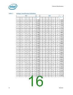
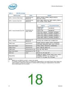
Table 2.
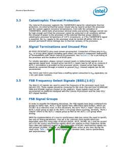
FSB Pin Groups
Signal Group
Type
Signals
Synchronous to
BCLK[1:0]
BPRI#, DEFER#, DPWR#, PREQ#, RESET#,
RS[2:0]#, TRDY#
AGTL+ Common Clock Input
AGTL+ Common Clock I/O
Synchronous to
BCLK[1:0]
ADS#, BNR#, BPM[3:0]#, BR0#, DBSY#, DRDY#,
HIT#, HITM#, LOCK#, PRDY#
Signals
REQ[4:0]#,
Associated Strobe
ADSTB[0]#
A[16:3]#
Synchronous to
assoc. strobe
A[31:17]#
ADSTB[1]#
AGTL+ Source Synchronous I/O
D[15:0]#, DINV0#
DSTBP0#, DSTBN0#
D[31:16]#, DINV1# DSTBP1#, DSTBN1#
D[47:32]#, DINV2# DSTBP2#, DSTBN2#
D[63:48]#, DINV3# DSTBP3#, DSTBN3#
Synchronous to
BCLK[1:0]
AGTL+ Strobes
CMOS Input
ADSTB[1:0]#, DSTBP[3:0]#, DSTBN[3:0]#
A20M#, DPSLP#, IGNNE#, INIT#, LINT0/INTR,
LINT1/NMI, PWRGOOD, SMI#, SLP#, STPCLK#
Asynchronous
Open Drain Output
CMOS Output
CMOS Input
Asynchronous
Asynchronous
Synchronous to TCK
Synchronous to TCK
Clock
FERR#, IERR#, PROCHOT#, THERMTRIP#
PSI#, VID[5:0], BSEL[1:0]
TCK, TDI, TMS, TRST#
TDO
Open Drain Output
FSB Clock
BCLK[1:0], ITP_CLK[1:0]2
COMP[3:0], DBR#2, GTLREF, RSVD, TEST2, TEST1,
THERMDA, THERMDC, VCC, VCCA[3:0], VCCP,
VCCQ[1:0], VCC_SENSE, VSS, VSS_SENSE
Power/Other
NOTES:
1.
2.
BPM[2:0}# and PRDY# are AGTL+ output only signals.
In processor systems where there is no debug port implemented on the system board, these signals are
used to support a debug port interposer. In systems with the debug port implemented on the system
board, these signals are no connects.
18
Datasheet

 INTEL [ INTEL ]