Processor Configuration Registers
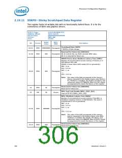
B/D/F/Type:
Address Offset:
Reset Value:
Access:
0/0/0/MCHBAR PCU
5D10–5D17h
0000000000000000h
RWS, RW
Size:
64 bits
Reset
Value
RST/
PWR
Bit
13:8
7:6
Access
Description
Self Refresh and MDLL Latency Time (WM1)
This field provides the number of microseconds to access
memory if memory is in Self Refresh and MDLL is turned off
(0.5 us granularity).
00h = 0 us
01h = 0.5 us
02h = 1 us
...
RWS
000000b
Powergood
3Fh = 31.5 us
Note: The value in this field corresponds to the memory
latency requested to the Display Engine when Memory
is in Self Refresh. The Display LP1 latency and
watermark values (GTTMMADR offset 45108h) should
be programmed to match the latency in this register.
Reserved for Future Use (RWSVD0)
RWS
00b
Powergood
Reserved for Future Use
Normal Latency Time (WM0)
This field provides the number of microseconds to access
memory for normal memory operations (0.1 us granularity).
00h = 0 us
01h = 0.1 us
02h = 0.2 us
...
3Fh = 6.3 us
Note: For the processor, the worst-case latency is 0.6 us.
5:0
RWS
000000b
Powergood WM0 latency is the sum of:
•
•
•
Partial Intel High Definition Audio request in front of the
Display Request = 100 ns
Refresh just in front of the Intel High Definition Audio
request = 300 ns
Maintenance (ZQCAL + some clocks) = 130 ns (DDR 1067)
to 80 ns (DDR 1600)
•
•
•
Activate = 15 ns
CAS = 15 ns
SA Roundtrip = ~15 ns
Total: 525 ns (DDR 1600) – 575 ns (DDR 1067)
Datasheet, Volume 2
307

 INTEL [ INTEL ]