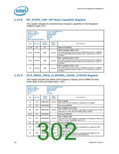
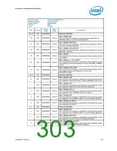
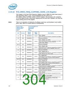
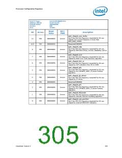
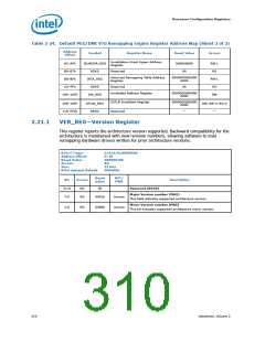
Processor Configuration Registers
2.19.11 SSKPD—Sticky Scratchpad Data Register
This register holds 64 writable bits with no functionality behind them. It is for the
convenience of BIOS and graphics drivers.
B/D/F/Type:
Address Offset:
Reset Value:
Access:
0/0/0/MCHBAR PCU
5D10–5D17h
0000000000000000h
RWS, RW
Size:
64 bits
Reset
Value
RST/
PWR
Bit
Access
Description
Scratchpad Data (SKPD)
63:32
RWS
00000000h Powergood
2 WORDs of data storage.
Reserved for Future Use (RWSVD3)
31:30
RWS
00b
Powergood Bit 30 controls the way BIOS calculate WM3 value.
Bit 31 is reserved for future use.
DDRIO Power down Shutdown Latency Time (WM3)
Number of microseconds to access memory if memory is in
Self Refresh (SR) with
DDRIO in Power down (EPG mode) (0.5 us granularity).
00h = 0 us
01h = 0.5 us
02h = 1 us
29:24
RWS
00h
Powergood
...
3Fh = 31.5 us
Note: The value in this field corresponds to the memory
latency requested to the Display Engine when Memory
PLL Shutdown is enabled. The Display LP3 latency and
watermark values (GTTMMADR offset 45110h) should
be programmed to match the latency in this register.
Reserved for Future Use (RWSVD2)
Powergood
23
22
RWS
RW
0b
0b
Reserved for Future Use
MPLL Fast Lock Disable (MPLL_FAST_DIS)
Uncore
Copy of CR PCU [SBPLL_FAST_DIS]
MPLL Shutdown Latency Time (WM2)
Number of microseconds to access memory if the MPLL is
shutdown (requires memory in Self Refresh). The value is
programmed in 0.5 us granularity.
00h = 0 us
01h = 0.5 us
02h = 1 us
21:16
RWS
000000b
Powergood
...
3Fh = 31.5 us
Note: The value in this field corresponds to the memory
latency requested to the Display Engine when MPLL
shutdown is enabled. The Display LP2 latency and
watermark values (GTTMMADR offset 4510Ch) should
be programmed to match the latency in this register.
Reserved for Future Use (RWSVD1)
Powergood
15:14
RWS
00b
Reserved for Future Use
306
Datasheet, Volume 2

 INTEL [ INTEL ]