Processor Configuration Registers
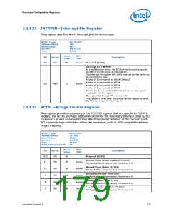
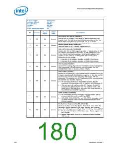
B/D/F/Type:
Address Offset:
Reset Value:
Access:
0/6/0/PCI
3E–3Fh
0000h
RO, RW
16 bits
0h
Size:
BIOS Optimal Default
Reset
Value
RST/
PWR
Bit
6
Access
RW
Description
Secondary Bus Reset (SRESET)
Setting this bit triggers a hot reset on the corresponding PCI
Express Port. This will force the LTSSM to transition to the Hot
Reset state (using Recovery) from L0, L0s, or L1 states.
0b
0b
Uncore
Uncore
Master Abort Mode (MAMODE)
Does not apply to PCI Express. Hardwired to 0.
5
RO
VGA 16-bit Decode (VGA16D)
Enables the PCI-to-PCI bridge to provide 16-bit decoding of VGA
I/O address precluding the decoding of alias addresses every
1 KB. This bit only has meaning if bit 3 (VGA Enable) of this
register is also set to 1, enabling VGA I/O decoding and
forwarding by the bridge.
0 = Execute 10-bit address decodes on VGA I/O accesses.
1 = Execute 16-bit address decodes on VGA I/O accesses.
4
3
RW
RW
0b
0b
Uncore
Uncore
VGA Enable (VGAEN)
Controls the routing of processor initiated transactions targeting
VGA compatible I/O and memory address ranges. See the
VGAEN/MDAP table in device 0, offset 97h[0].
ISA Enable (ISAEN)
Needed to exclude legacy resource decode to route ISA resources
to legacy decode path. Modifies the response by the root port to
an I/O access issued by the processor that target ISA I/O
addresses. This applies only to I/O addresses that are enabled by
the IOBASE and IOLIMIT registers.
0 = All addresses defined by the IOBASE and IOLIMIT for
processor I/O transactions will be mapped to PCI Express-G.
2
RW
0b
Uncore
1 = The root port will not forward to PCI Express-G any I/O
transactions addressing the last 768 bytes in each 1 KB
block even if the addresses are within the range defined by
the IOBASE and IOLIMIT registers.
SERR Enable (SERREN)
0 = No forwarding of error messages from secondary side to
primary side that could result in an SERR.
1 = ERR_COR, ERR_NONFATAL, and ERR_FATAL messages result
in SERR message when individually enabled by the Root
Control register.
1
0
RW
RW
0b
0b
Uncore
Uncore
Parity Error Response Enable (PEREN)
Controls whether or not the Master Data Parity Error bit in the
Secondary Status register is set when the root port receives
across the link (upstream) a Read Data Completion Poisoned TLP
0 = Master Data Parity Error bit in Secondary Status register can
NOT be set.
1 = Master Data Parity Error bit in Secondary Status register
CAN be set.
180
Datasheet, Volume 2

 INTEL [ INTEL ]