Processor Configuration Registers
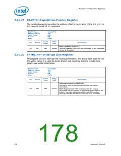
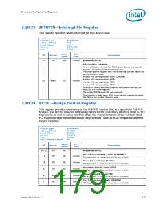
2.10.23 INTRPIN—Interrupt Pin Register
This register specifies which interrupt pin this device uses.
B/D/F/Type:
Address Offset:
Reset Value:
Access:
0/6/0/PCI
3Dh
01h
RW-O, RO
8 bits
Size:
Reset
Value
RST/
PWR
Bit
Access
Description
7:3
RO
00h
Uncore
Reserved (RSVD)
Interrupt Pin (INTPIN)
As a multifunction device, the PCI Express device may specify
any INTx (x=A,B,C,D) as its interrupt pin.
The Interrupt Pin register tells which interrupt pin the device (or
device function) uses.
A value of 1 corresponds to INTA# (Default)
A value of 2 corresponds to INTB#
A value of 3 corresponds to INTC#
A value of 4 corresponds to INTD#
2:0
RW-O
1h
Uncore
Devices (or device functions) that do not use an interrupt pin
must put a 0 in this register.
The values 05h through FFh are reserved.
This register is write once. BIOS must set this register to select
the INTx to be used by this root port.
2.10.24 BCTRL—Bridge Control Register
This register provides extensions to the PCICMD register that are specific to PCI-PCI
bridges. The BCTRL provides additional control for the secondary interface (that is, PCI
Express-G) as well as some bits that affect the overall behavior of the "virtual" Host-
PCI Express bridge embedded within the processor; such as VGA compatible address
ranges mapping.
B/D/F/Type:
Address Offset:
Reset Value:
Access:
0/6/0/PCI
3E–3Fh
0000h
RO, RW
16 bits
0h
Size:
BIOS Optimal Default
Reset
Value
RST/
PWR
Bit
15:12
11
Access
RO
Description
0h
0b
Reserved (RSVD)
Discard Timer SERR# Enable (DTSERRE)
Not Applicable or Implemented. Hardwired to 0.
RO
Uncore
Uncore
Uncore
Uncore
Uncore
Discard Timer Status (DTSTS)
Not Applicable or Implemented. Hardwired to 0.
10
9
RO
RO
RO
RO
0b
0b
0b
0b
Secondary Discard Timer (SDT)
Not Applicable or Implemented. Hardwired to 0.
Primary Discard Timer (PDT)
Not Applicable or Implemented. Hardwired to 0.
8
Fast Back-to-Back Enable (FB2BEN)
Not Applicable or Implemented. Hardwired to 0.
7
Datasheet, Volume 2
179

 INTEL [ INTEL ]