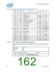
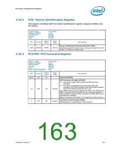
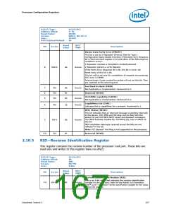
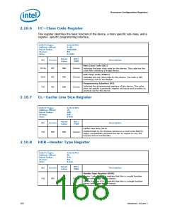
Processor Configuration Registers
B/D/F/Type:
Address Offset:
Reset Value:
Access:
0/6/0/PCI
4–5h
0000h
RW, RO
16 bits
00h
Size:
BIOS Optimal Default
Reset
Value
RST/
PWR
Bit
Access
Description
Bus Master Enable (BME)
THis bit controls the ability of the PEG port to forward Memory
Read/Write Requests in the upstream direction.
0 = This device is prevented from making memory requests to
its primary bus. According to PCI Specification, as MSI
interrupt messages are in-band memory writes, disabling
the bus master enable bit prevents this device from
generating MSI interrupt messages or passing them from its
secondary bus to its primary bus. Upstream memory
writes/reads, peer writes/reads, and MSIs will all be treated
as illegal cycles. Writes are aborted. Reads are aborted and
will return Unsupported Request status (or Master abort) in
its completion packet
2
RW
0b
Uncore
1 = This device is allowed to issue requests to its primary bus.
Completions for previously issued memory read requests on
the primary bus will be issued when the data is available.
This bit does not affect forwarding of Completions from the
primary interface to the secondary interface.
Memory Access Enable (MAE)
0 = All of device's memory space is disabled.
1
0
RW
RW
0b
0b
Uncore
Uncore
1 = Enable the Memory and Pre-fetchable memory address
ranges defined in the MBASE, MLIMIT, PMBASE, and
PMLIMIT registers.
IO Access Enable (IOAE)
0 = All of device’s I/O space is disabled.
1 = Enable the I/O address range defined in the IOBASE, and
IOLIMIT registers.
Datasheet, Volume 2
165

 INTEL [ INTEL ]