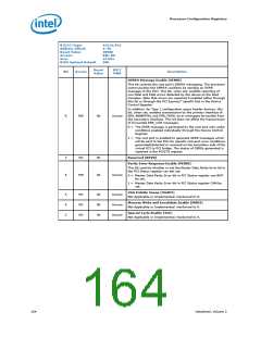
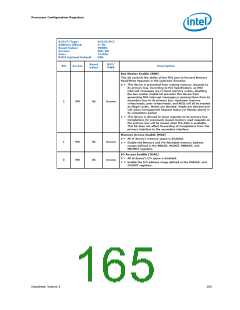
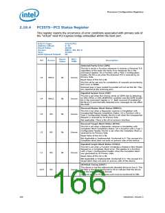
Processor Configuration Registers
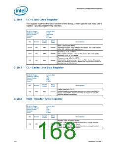
2.10.6
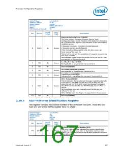
CC—Class Code Register
This register identifies the basic function of the device, a more specific sub-class, and a
register- specific programming interface.
B/D/F/Type:
Address Offset:
Reset Value:
Access:
0/6/0/PCI
9–Bh
060400h
RO
Size:
24 bits
Reset
Value
RST/
PWR
Bit
Access
Description
Base Class Code (BCC)
23:16
RO
06h
04h
Uncore
Uncore
Indicates the base class code for this device. This code has the
value 06h indicating a Bridge device.
Sub-Class Code (SUBCC)
Indicates the sub-class code for this device. The code is 04h
indicating a PCI to PCI Bridge.
15:8
7:0
RO
RO
Programming Interface (PI)
Indicates the programming interface of this device. This value
does not specify a particular register set layout and provides no
practical use for this device.
00h
Uncore
2.10.7
CL—Cache Line Size Register
B/D/F/Type:
Address Offset:
Reset Value:
Access:
0/6/0/PCI
Ch
00h
RW
8 bits
Size:
Reset
Value
RST/
PWR
Bit
Access
Description
Cache Line Size (CLS)
Implemented by PCI Express devices as a read-write field for
legacy compatibility purposes but has no impact on any PCI
Express device functionality.
7:0
RW
00h
Uncore
2.10.8
HDR—Header Type Register
B/D/F/Type:
Address Offset:
Reset Value:
Access:
0/6/0/PCI
Eh
81h
RO
8 bits
Size:
Reset
Value
RST/
PWR
Bit
Access
Description
Header Type Register (HDR)
Device 1 returns 81h to indicate that this is a multi function
device with bridge header layout.
7:0
RO
81h
Uncore
Device 6 returns 01h to indicate that this is a single function
device with bridge header layout.
168
Datasheet, Volume 2

 INTEL [ INTEL ]