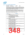
Chipset Configuration Registers
10.1.79 FDSW—Function Disable SUS Well
Offset Address: 3420h
Attribute:
Size:
R/W
8-bit
Default Value:
00h
Bit
Description
Function Disable SUS Well Lockdown (FDSWL)— R/W
0 = FDSW registers are not locked down
1 = FDSW registers are locked down
7
6:0
Reserved
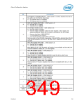
10.1.80 CIR8—Chipset Initialization Register 8
Offset Address: 3430-3433h
Attribute:
Size:
R/W
32-bit
Default Value:
00000000h
Bit
Description
7:2
1:0
Reserved
CIR8 Field 1 — R/W. BIOS must program this field to 10b.
10.1.81 CIR9—Chipset Initialization Register 9
Offset Address: 350Ch–350Fh
Attribute:
Size:
R/W
32-bit
Default Value:
00000000h
Bit
Description
31:28
27:26
25:0
Reserved
CIR9 Field 1 — R/W. BIOS must program this field to 10b.
Reserved
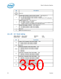
10.1.82 PPO—Port Power Off
Offset Address: 3524–3525h
Attribute:
Size:
R/W
16-bit
Default Value:
0000h
Bit
Description
15:12
11:0
Reserved
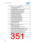
USB Port Power Off— R/W
1 = The corresponding EHCI and UHCI ports are electrically disconnected in this
mode.
Warning:
The platform must ensure that the powered off ports are not routed
to any internal USB header or external USB connector. The ICH
provides pull-down termination resistors.
This register can not be written when the USB Per-Port Registers Write Enable bit
(UPRWC register, PMBASE + 3C, bit 1) is 0.
352
Datasheet

 INTEL [ INTEL ]