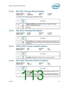
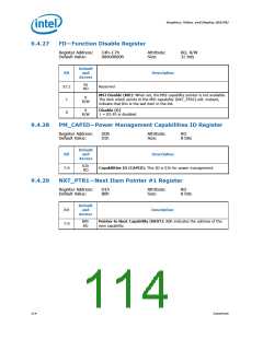
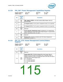
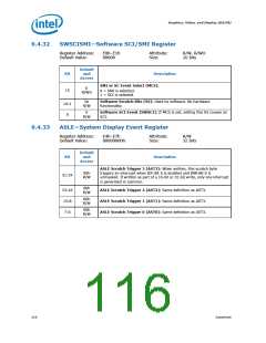
Graphics, Video, and Display (D2:F0)
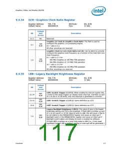
9.4.34
GCR—Graphics Clock Ratio Register
Register Address:
Default Value:
F0h–F3h
00000002h
Attribute:
Size:
RO, R/W
32 bits
c
Default
Bit
and
Description
Access
31:2
RO
Reserved
Graphics 2x Clock to Graphics Clock Ratio: The field is used to
configure the graphics 2-D processing engine.
10b
R/W
3:2
1:0
01 = ratio is 2:1
All other encodings are reserved.
Graphics Clock to Core Clock Ratio (GCCR): Set by BIOS to correctly
configure the graphics clock frequency as a function of the Intel SCH core
clock frequency.
01 = ratio is 2:1 for:
10b
R/W
200 MHz Graphics at 100 MHz FSB operation
266 MHz Graphics at 133 MHz FSB operation
10 = ratio is 3:2 for:
200 MHz Graphics at 133-MHz FSB operation
All other encodings are reserved.
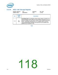
9.4.35
LBB—Legacy Backlight Brightness Register
Register Address:
Default Value:
F4h–F7h
00000000h
Attribute:
Size:
RO, R/W
32 bits
Default
Bit
and
Description
Access
LBPC Scratch Trigger 3 (LST3): When enabled by internal register bits,
a write to this range triggers an display event interrupt. If written as part
of a 16-bit or 32-bit write, only one interrupt is generated in common.
00h
R/W
31:24
00h
R/W
23:16
15:8
LBPC Scratch Trigger 2 (LST2): Same definition as LST3
LBPC Scratch Trigger 1 (LST1): Same definition as LST3
00h
R/W
Legacy Backlight Brightness (LBES): The value of zero is the lowest
brightness setting and 255 is the brightest. If field LBES is written as part
of a 16-bit (word) or 32-bit (dword) write to LBB, this will cause a flag to
be set (LBES) in the PIPEBSTATUS register and cause an interrupt if
Backlight event in the PIPEBSTATUS register and cause an Interrupt if
Backlight Event (LBEE) and Display B Event is enabled by software.
00h
R/W
7:0
(If field LBES is written as a (one) byte write to LBB (i.e., if only least
significant byte of LBB is written), no flag or interrupt will be generated.)
Datasheet
117

 INTEL [ INTEL ]