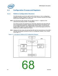
GMCH Register Description
The GMCH contains three PCI devices within a single physical component. The
configuration registers for the three devices are mapped as devices residing on PCI
bus 0.
•
Device 0: Host Bridge/DRAM Controller. Logically this appears as a PCI device
residing on PCI bus 0. Device 0 contains the standard PCI header registers, PCI
Express base address register, DRAM control, and configuration for the DMI and
other GMCH specific registers.
•
Device 1: Host-PCI Express Bridge. Logically this appears as a “virtual” PCI-to-
PCI bridge residing on PCI bus 0 and is compliant with PCI Express* Specification
Rev 1.1. Device 1 contains the standard PCI-to-PCI bridge registers and the
standard PCI Express/PCI configuration registers (including the PCI Express
memory address mapping). It also contains Isochronous and Virtual Channel
controls in the PCI Express extended configuration space.
•
•
Device 2: Internal Graphics Control. Logically, this appears as a PCI device
residing on PCI bus 0. Physically, device 2 contains the configuration registers for
3D, 2D, and display functions.
Device 3: Manageability Engine Device. Logically, this appears as a PCI device
residing on PCI bus 0. Physically, device 3.
4.3
Configuration Mechanisms
The processor is the originator of configuration cycles so the FSB is the only interface
in the platform where these mechanisms are used. Internal to the GMCH transactions
received through both configuration mechanisms are translated to the same format.
4.3.1
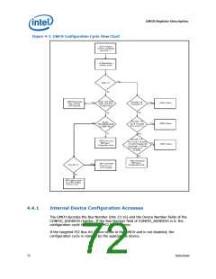
Standard PCI Configuration Mechanism
The following is the mechanism for translating processor I/O bus cycles to
configuration cycles.
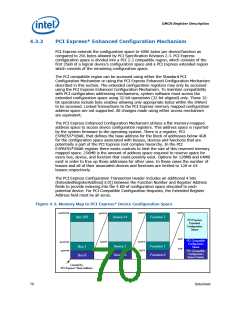
The PCI specification defines a slot based "configuration space" that allows each
device to contain up to 8 functions with each function containing up to 256 8-bit
configuration registers. The PCI specification defines two bus cycles to access the PCI
configuration space: Configuration Read and Configuration Write. Memory and I/O
spaces are supported directly by the processor. Configuration space is supported by a
mapping mechanism implemented within the GMCH.
The configuration access mechanism makes use of the CONFIG_ADDRESS Register (at
I/O address 0CF8h though 0CFBh) and CONFIG_DATA Register (at I/O address 0CFCh
though 0CFFh). To reference a configuration register a DW I/O write cycle is used to
place a value into CONFIG_ADDRESS that specifies the PCI bus, the device on that
bus, the function within the device and a specific configuration register of the device
function being accessed. CONFIG_ADDRESS[31] must be 1 to enable a configuration
cycle. CONFIG_DATA then becomes a window into the four bytes of configuration
space specified by the contents of CONFIG_ADDRESS. Any read or write to
CONFIG_DATA will result in the GMCH translating the CONFIG_ADDRESS into the
appropriate configuration cycle.
The GMCH is responsible for translating and routing the processor’s I/O accesses to
the CONFIG_ADDRESS and CONFIG_DATA registers to internal GMCH configuration
registers, DMI or PCI Express.
Datasheet
69

 INTEL [ INTEL ]