Intel® Celeron® Processor for PGA370 up to 1.40 GHz on 0.13 µ Process
1.0
Introduction
The Intel® Celeron® processor based on 0.13 micron process core for the PGA370 socket is the
next member of the P6 family, in the Intel IA-32 processor line and hereafter will be referred to as
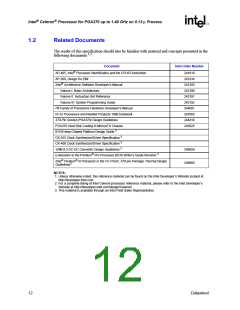
simply “the processor”. The processor will continue in the package technology called flip-chip pin
grid array but will contain a Integrated Heat Spreader (IHS) (see Figure 1). The flip-chip with IHS
package will be labeled as FC-PGA2 and will utilize the same 370-pin zero insertion force socket
(PGA370). Thermal solutions contact the IHS directly for the FC-PGA2 package and not to the
bare-die as with the FC-PGA attachment.
The processor, like its predecessors in the P6 family of processors, implements a Dynamic
Execution microarchitecture—a unique combination of multiple branch prediction, data flow
analysis, and speculative execution. The processor delivers higher performance than the Intel®
Celeron® processor based on 0.18 micron process core, while maintaining binary compatibility
with all previous Intel Architecture processors. The processor also executes Intel® MMXTM
technology instructions for enhanced media and communication performance just as the
predecessor Celeron processor based on 0.18 micron process core. Additionally, the processor
executes Streaming SIMD (single-instruction, multiple data) Extensions for enhanced floating
point and 3-D application performance. The processor utilizes multiple low-power states such as
Stop-Grant, Sleep, and Deep Sleep to conserve power during idle times.
The processor includes an integrated on-die, 256KB 8-way set associative level-two (L2) cache.
The L2 cache implements the Advanced Transfer Cache Architecture with a 256-bit wide bus. The
processor also includes a 16 KB level one (L1) instruction cache and 16 KB L1 data cache. These
cache arrays run at the full speed of the processor core. The processor for the PGA370 socket has a
dedicated L2 cache bus, thus maintaining the dual independent bus architecture to deliver high bus
bandwidth and performance. Memory is cacheable for 64 GB of addressable memory space,
allowing significant headroom for desktop systems. Refer to the Specification Update document
for this processor to determine the cacheability and cache configuration options for a specific
processor. Contact your nearest Intel Sales Representative for the latest Processor Specification
Update.
Figure 1. Integrated Heat Spreader (IHS)
FC-PGA2 w/IHS
FC-PGA
The processor will support a lower voltage differential and single-ended clocking for the system
bus. The previous generation Intel Celeron processors for the PGA370 socket will function in a
platform that supports this processor, if the platform has been designed to be backward compatible.
In addition, the processor will not function in a previous generation platform due to incompatible
system bus signal levels and clock type. Care must be taken to ensure the correct processors are
installed in the correct PGA370 socket platforms.
Datasheet
9

 INTEL [ INTEL ]