Ultra-Low Voltage Intel® Celeron® Processor — 650 MHz and 400 MHz
4.3.1.1
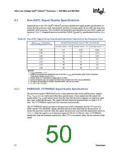
VTTPWRGD Noise Parameter Specification
Table 35. VTTPWRGD Noise Parameter Specification
Parameter
Specification
Amount of noise (glitch)
Less than 100 mV
In addition, the VTTPWRGD signal should have reasonable transition time through the transition
region. A sharp edge on the signal transition will minimize the chance of noise causing a glitch on
this signal. Intel recommends the following transition time for the VTTPWRGD signal.
4.3.1.2
VTTPWRGD Transition Parameter Recommendation
Table 36. VTTPWRGD Transition Parameter Recommendation
Parameter
Recommendation
Transition time (300 mV to 900 mV)
Less than or equal to 100 µs
In addition, the VTT_PWRGD signal should have reasonable transition time through the transition
region. A sharp edge on the signal transition will minimize the chance of noise causing a glitch on
this signal. Intel recommends the following transition time for the VTT_PWRGD signal.
4.3.1.2.1 Transition Region
The transition region covered by this requirement is 300 mV to 900 mV. Once the VTTPWRGD
signal is in that voltage range, the processor is more sensitive to noise, which may be present on the
signal. The transition region when the signal first crosses the 300-mV voltage level and continues
until the last time it is below 900 mV.
4.3.1.2.2 Transition Time
The transition time is defined as the time the signal takes to move through the transition region. A
100-µs transition time will ensure that the processor receives a good transition edge.
4.3.1.2.3 Noise
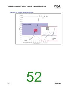
The signal quality of the VTTPWRGD signal is critical to the correct operation of the processor.
Every effort should be made to ensure this signal is monotonic in the transition region. If noise or
glitches are present on this signal, the noise or glitches must be kept to less than 100 mV of a
voltage drop from the highest voltage level received to that point. This glitch must remain less than
100 mV until the excursion ends by the voltage returning to the highest voltage previously
received. See Figure 21 for an example graph of this situation and requirements.
Datasheet
51

 INTEL [ INTEL ]