XMC4500
XMC4000 Family
Electrical Parameters
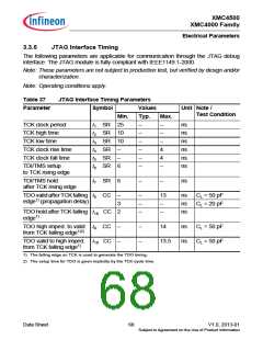
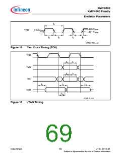
3.3.6
JTAG Interface Timing
The following parameters are applicable for communication through the JTAG debug
interface. The JTAG module is fully compliant with IEEE1149.1-2000.
Note: These parameters are not subject to production test, but verified by design and/or
characterization.
Note: Operating conditions apply.
Table 37
JTAG Interface Timing Parameters
Symbol Values
Parameter
Unit Note /
Test Condition
Min.
Typ.
Max.
TCK clock period
TCK high time
t1 SR 25
t2 SR 10
t3 SR 10
–
–
–
–
–
–
–
–
–
4
4
–
ns
ns
ns
ns
ns
ns
TCK low time
TCK clock rise time
TCK clock fall time
t4 SR
t5 SR
t6 SR
–
–
6
TDI/TMS setup
to TCK rising edge
TDI/TMS hold
t7 SR
6
–
–
ns
after TCK rising edge
TDO valid after TCK falling t8 CC
–
3
2
–
–
–
13
–
ns
ns
ns
CL = 50 pF
CL = 20 pF
edge1) (propagation delay)
TDO hold after TCK falling t18 CC
–
edge1)
TDO high imped. to valid t9 CC
–
–
–
–
14
ns
ns
CL = 50 pF
CL = 50 pF
from TCK falling edge1)2)
TDO valid to high imped. t10 CC
13.5
from TCK falling edge1)
1) The falling edge on TCK is used to generate the TDO timing.
2) The setup time for TDO is given implicitly by the TCK cycle time.
Data Sheet
68
V1.0, 2013-01
Subject to Agreement on the Use of Product Information

 INFINEON [ Infineon ]