XMC4500
XMC4000 Family
Electrical Parameters
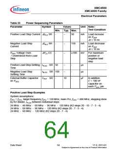
Table 33
Power Sequencing Parameters
Symbol
Parameter
Values
Unit Note /
Test Condition
Min. Typ. Max.
Positive Load Step Current ΔIPLS SR
-
-
-
−
−
−
50
mA Load increase
on VDDP
Δt ≤ 10 ns
Negative Load Step
Current
ΔINLS SR
ΔVLS CC
150
±100
mA Load decrease
on VDDP
Δt ≤ 10 ns
V
DDC Voltage Over-
mV For maximum
positive or
/ Undershoot from Load
Step
negative load
step
Positive Load Step Settling tPLSS SR 50
Time
−
-
-
-
μs
μs
Negative Load Step
Settling Time
tNLSS SR 100
CEXT SR
−
External Buffer Capacitor
-
10
μF
In addition
on VDDC
C = 100 nF
capacitor on
each VDDC pin
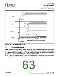
Positive Load Step Examples
System assumptions:
f
CPU = fSYS, target frequency fCPU = 120 MHz, main PLL fVCO = 480 MHz, stepping done
by K2 divider, tPLSS between individual steps:
24 MHz - 48 MHz - 68 MHz - 96 MHz - 120 MHz (K2 steps 20 - 10 - 7 - 5 - 4)
24 MHz - 68 MHz - 96 MHz - 120 MHz (K2 steps 20 - 7 - 5 - 4)
24 MHz - 68 MHz - 120 MHz (K2 steps 20 - 7 - 4)
Data Sheet
64
V1.0, 2013-01
Subject to Agreement on the Use of Product Information

 INFINEON [ Infineon ]