XC2287 / XC2286 / XC2285
XC2000 Family Derivatives
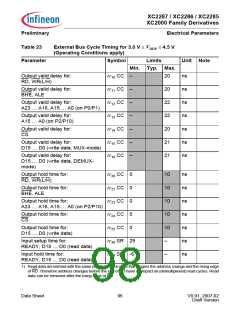
Preliminary
Electrical Parameters
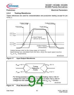
4.4.4
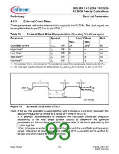
Testing Waveforms
These references are used for characterization and production testing (except for pin
XTAL1).
Output delay
Hold time
Output delay
Hold time
0.8 VDDP
0.7 VDDP
Input Signal
(driven by tester)
0.3 VDDP
0.2 VDDP
Output Signal
(measured)
Output timings refer to the rising edge of CLKOUT.
Input timings are calculated from the time, when the input signal reaches
VIH or VIL, respectively.
MCD05556C
Figure 17
Input Output Waveforms
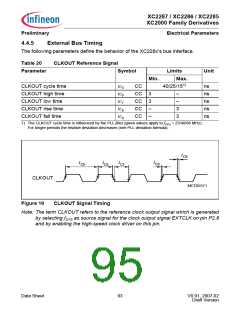
V
Load + 0.1 V
V
V
OH - 0.1 V
OL + 0.1 V
Timing
Reference
Points
V
Load - 0.1 V
For timing purposes a port pin is no longer floating when a 100 mV
change from load voltage occurs, but begins to float when a 100 mV
change from the loaded VOH /VOL level occurs (IOH / IOL = 20 mA).
MCA05565
Figure 18
Float Waveforms
Data Sheet
92
V0.91, 2007-02
Draft Version

 INFINEON [ Infineon ]