XC2287 / XC2286 / XC2285
XC2000 Family Derivatives
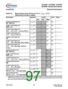
Preliminary
Electrical Parameters
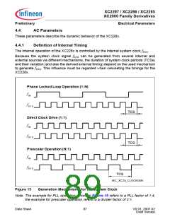
4.4.3
External Clock Drive
These parameters define the external clock supply for the XC228x. The clock signal can
be supplied either to pin P2.9 or to pin XTAL1.
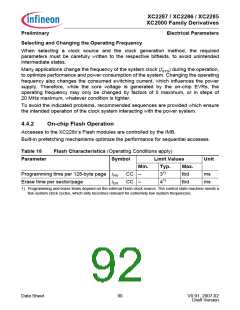
Table 19
External Clock Drive Characteristics (Operating Conditions apply)
Parameter
Symbol
Limit Values
Unit
Min.
25
6
Max.
2501)
Oscillator period
High time2)
Low time2)
Rise time2)
Fall time2)
tOSC
t1
SR
SR
SR
SR
SR
ns
ns
ns
ns
ns
–
–
8
8
t2
6
t3
–
t4
–
1) The maximum limit is only relevant for PLL operation to ensure the minimum input frequency for the PLL.
2) The clock input signal must reach the defined levels VILC and VIHC (for XTAL1) or VIL and VIH for P2.9.
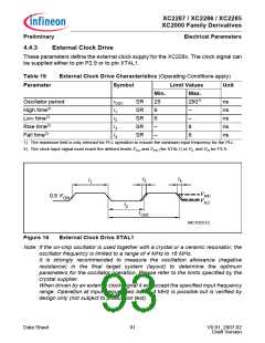
t3
t4
t1
VIHC
VILC
0.5 VDDI
t2
tOSC
MCT05572
Figure 16
External Clock Drive XTAL1
Note: If the on-chip oscillator is used together with a crystal or a ceramic resonator, the
oscillator frequency is limited to a range of 4 MHz to 16 MHz.
It is strongly recommended to measure the oscillation allowance (negative
resistance) in the final target system (layout) to determine the optimum
parameters for the oscillator operation. Please refer to the limits specified by the
crystal supplier.
When driven by an external clock signal it will accept the specified input frequency
range. Operation at input frequencies below 4 MHz is possible but is verified by
design only (not subject to production test).
Data Sheet
91
V0.91, 2007-02
Draft Version

 INFINEON [ Infineon ]