XC2287 / XC2286 / XC2285
XC2000 Family Derivatives
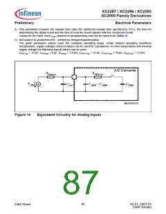
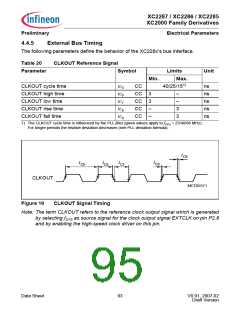
Preliminary
Electrical Parameters
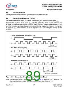
The timing listed in the AC Characteristics refers to TCSs. Therefore, the timing must be
calculated using the minimum TCS possible under the respective circumstances.
The actual minimum value for TCS depends on the jitter of the PLL. As the PLL is
constantly adjusting its output frequency so it corresponds to the applied input frequency
(crystal or oscillator), the accumulated jitter is limited, which means that the relative
deviation for periods of more than one TCS is lower than for one single TCS.
This is especially important for bus cycles using waitstates and e.g. for the operation of
timers, serial interfaces, etc. For all slower operations and longer periods (e.g. pulse train
generation or measurement, lower baudrates, etc.) the deviation caused by the PLL jitter
is, therefore, negligible.
The value of the accumulated PLL jitter depends on the number of consecutive VCO
output cycles within the respective timeframe. The VCO output clock is divided by the
output prescaler (K2+1) to generate the system clock signal fSYS. Therefore, the number
of VCO cycles can be represented as (K2+1) × T, where T is the number of consecutive
f
SYS cycles (TCS).
Different frequency bands can be selected for the VCO, so the operation of the PLL can
be adjusted to a wide range of input and output frequencies:
Table 17
PLLCON0.VCOSEL VCO Frequency Range
VCO Bands for PLL Operation1)
Base Frequency Range
10 … 40 MHz
00
01
1X
40 … 120 MHz
90 … 160 MHz
Reserved
20 … 80 MHz
1) Not subject to production test - verified by design/characterization.
Wakeup Oscillator
When wakeup oscillator operation is configured (SYSCON0.CLKSEL = 00B), the system
clock is derived from the low-frequency wakeup oscillator:
f
SYS = fWU.
In this mode, a basic functionality can be maintained without requiring an external clock
source and while minimizing the power consumption.
Data Sheet
89
V0.91, 2007-02
Draft Version

 INFINEON [ Infineon ]