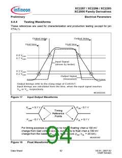
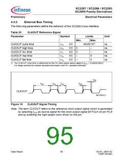
XC2287 / XC2286 / XC2285
XC2000 Family Derivatives
Preliminary
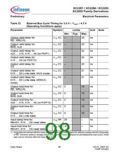
Table 23
Electrical Parameters
External Bus Cycle Timing for 3.0 V ≤ VDDP ≤ 4.5 V
(Operating Conditions apply)
Parameter
Symbol
Limits
Unit Note
Min. Typ. Max.
Output valid delay for:
RD, WR(L/H)
tc10 CC –
20
20
22
22
20
21
21
ns
ns
ns
ns
ns
ns
ns
Output valid delay for:
BHE, ALE
tc11 CC –
tc12 CC –
tc13 CC –
tc14 CC –
tc15 CC –
tc16 CC –
Output valid delay for:
A23 … A16, A15 … A0 (on P0/P1)
Output valid delay for:
A15 … A0 (on P2/P10)
Output valid delay for:
CS
Output valid delay for:
D15 … D0 (write data, MUX-mode)
Output valid delay for:
D15 … D0 (write data, DEMUX-
mode)
Output hold time for:
RD, WR(L/H)
tc20 CC 0
tc21 CC 0
tc23 CC 0
tc24 CC 0
tc25 CC 0
tc30 SR 29
tc31 SR -6
10
10
10
10
10
–
ns
ns
ns
ns
ns
ns
ns
Output hold time for:
BHE, ALE
Output hold time for:
A23 … A16, A15 … A0 (on P2/P10)
Output hold time for:
CS
Output hold time for:
D15 … D0 (write data)
Input setup time for:
READY, D15 … D0 (read data)
Input hold time for:
–
READY, D15 … D0 (read data)1)
1) Read data are latched with the same (internal) clock edge that triggers the address change and the rising edge
of RD. Therefore address changes before the end of RD have no impact on (demultiplexed) read cycles. Read
data can be removed after the rising edge of RD.
Data Sheet
96
V0.91, 2007-02
Draft Version

 INFINEON [ Infineon ]