XC2287 / XC2286 / XC2285
XC2000 Family Derivatives
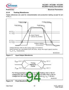
Preliminary
Electrical Parameters
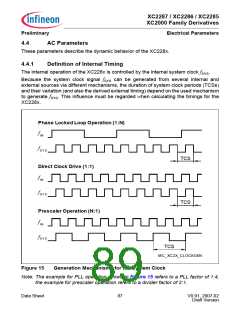
The specification of the external timing (AC Characteristics) depends on the period of the
system clock (TCS).
Direct Drive
When direct drive operation is configured (SYSCON0.CLKSEL = 11B), the system clock
is derived directly from the input clock signal DIRIN:
f
SYS = fIN.
The frequency of fSYS directly follows the frequency of fIN. In this case, the high and low
time of fSYS is defined by the duty cycle of the input clock fIN.
A similar configuration can be achieved by selecting the XTAL11) input.
Prescaler Operation
When prescaler operation is configured (SYSCON0.CLKSEL = 10B, PLLCON0.VCOBY
= 1B), the system clock is derived either from the crystal oscillator (input clock signal
XTAL1) or from the internal oscillator through the output-prescaler:
f
SYS = fOSC / (K1DIV + 1).
If the divider factor is selected as 1, the frequency of fSYS directly follows the frequency
of fOSC. In this case, the high and low time of fSYS is defined by the duty cycle of the input
clock fOSC (external or internal).
The lowest system clock frequency can be achieved in this mode by selecting the
maximum value for divider factor K1:
f
SYS = fOSC / 1024.
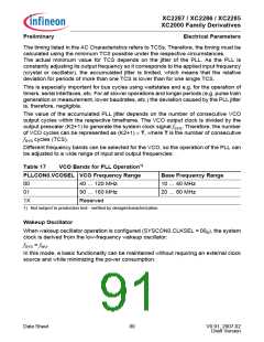
Phase Locked Loop (PLL)
When PLL operation is configured (SYSCON0.CLKSEL = 10B, PLLCON0.VCOBY = 0B),
the on-chip phase locked loop provides the system clock. The PLL multiplies the
selected input frequency by the factor F (fSYS = fIN × F), which results from the input
divider (P), the multiplication factor (N), and the output divider (K2): (F = N+1 / (P+1 ×
K2+1)).
The input clock can be derived either from an external source via XTAL1 or from the on-
chip oscillator.
The PLL circuit synchronizes the system clock to the input clock. This synchronization is
done smoothly, i.e. the system clock frequency does not change abruptly.
Due to this adaptation to the input clock the frequency of fSYS is constantly adjusted so it
is locked to fIN. The slight variation causes a jitter of fSYS which also affects the duration
of individual TCSs.
1) Voltages on XTAL1 must comply to the core supply voltage VDDI1
.
Data Sheet
88
V0.91, 2007-02
Draft Version

 INFINEON [ Infineon ]