XC2287 / XC2286 / XC2285
XC2000 Family Derivatives
Preliminary
Electrical Parameters
4.3
Analog/Digital Converter Parameters
These parameters describe how the optimum ADC performance can be reached.
Table 15
A/D Converter Characteristics (Operating Conditions apply)
Parameter
Symbol
Limit Values
Max.
Unit Test
Condition
Min.
1)
Analog reference supply
VAREF SR VAGND
VDDPA
+ 0.05
V
V
+ 1.0
Analog reference ground VAGND SR VSS
- 0.05
SR VAGND
0.5
VAREF
- 1.0
–
2)
3)
Analog input voltage range VAIN
Basic clock frequency
VAREF
V
fADCI
16.5
MHz
–
Conversion time for 10-bit tC10
CC (17 + STC) × tADCI
–
–
result4)
Conversion time for 8-bit tC8
CC (15 + STC) × tADCI
–
result4)
1)
5)
Total unadjusted error
TUE
CC –
±2
LSB
pF
Total capacitance
of an analog input
CAINT CC –
15
5)
5)
5)
5)
5)
Switched capacitance
of an analog input
CAINS CC –
7
pF
kΩ
pF
pF
kΩ
Resistance of
the analog input path
RAIN
CC –
1.5
20
20
2
Total capacitance
of the reference input
CAREFT CC –
CAREFS CC –
RAREF CC –
Switched capacitance
of the reference input
Resistance of
the reference input path
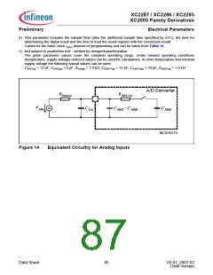
1) TUE is tested at VAREFx = VDDPA, VAGND = 0 V. It is verified by design for all other voltages within the defined
voltage range.
The specified TUE is valid only, if the absolute sum of input overload currents on Port 5 or Port 15 pins (see
I
OV specification) does not exceed 10 mA, and if VAREF and VAGND remain stable during the respective period
of time.
2) VAIN may exceed VAGND or VAREFx up to the absolute maximum ratings. However, the conversion result in these
cases will be X000H or X3FFH, respectively.
3) The limit values for fADCI must not be exceeded when selecting the peripheral frequency and the prescaler
setting.
Data Sheet
84
V0.91, 2007-02
Draft Version

 INFINEON [ Infineon ]