TLE9879QXA40
Electrical Characteristics
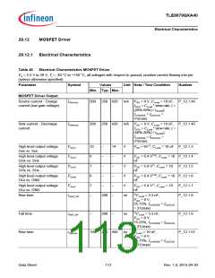
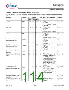
Table 40
Electrical Characteristics MOSFET Driver (cont’d)
VS = 5.5 V to 28 V, Tj = -40 °C to +150 °C, all voltages with respect to ground, positive current flowing into pin
(unless otherwise specified)
Parameter
Symbol
Values
Unit Note / Test Condition
Number
Min. Typ. Max.
Fall time
tfallmax
100
250 450
ns
µs
µs
ns
ns
C
Load = 10 nF,
P_12.1.58
V
SD > 8 V,
75-25%, ICHARGE = IDISCHG
= 31(max)
2)CLoad = 10 nF,
Rise time
Fall time
trisemin
1.25 2.5
1.25 2.5
5
P_12.1.14
P_12.1.15
P_12.1.35
P_12.1.36
P_12.1.11
V
SD > 8 V,
25-75%,
CHARGE = IDISCHG = 3(min)
2)CLoad = 10 nF,
SD > 8 V,
75-25%,
CHARGE = IDISCHG = 3(min)
Load = 10 nF,
SD > 8 V,
I
tfallmin
5
V
I
Absolute rise - fall time
difference for all LSx
tr_f(diff)LSx
–
–
–
–
100
100
C
V
25-75%, ICHARGE = IDISCHG
= 31(max)
Absolute rise - fall time
difference for all HSx
tr_f(diff)HSx
CLoad = 10 nF,
V
SD > 8 V,
25-75%, ICHARGE = IDISCHG
= 31(max)
2)
Resistor between GHx/GLx RGGND
and GND
30
30
40
40
50
50
kꢀ
kꢀ
–
Resistor between SHx and
GND
RSHGN
2)3) This resistance is the P_12.1.10
resistance between GHx
and GND connected
through a diode to SHx. As
a consequence, the
voltage at SHx can rise up
to 0,6V typ. before it is
discharged through the
resistor.
Low RDSON mode
(boosted discharge mode)
RONCCP
–
9
12
ꢀ
V
V
VSD = 13.5 V,
VCP = VVSD + 14.0 V;
P_12.1.50
I
CHARGE = IDISCHG =
31(max); 50mA forced into
Gx, Sx grounded
2)
Resistance between VDH
and VSD
IBSH
–
–
4
–
3
kꢀ
P_12.1.24
P_12.1.37
Input propagation time (LS
on)
tP(ILN)min
1.5
µs
C = 10 nF, (25%) /
tSLEWon
2)4)
Data Sheet
114
Rev. 1.0, 2015-04-30

 INFINEON [ Infineon ]