TLE9879QXA40
Electrical Characteristics
29.13
Operational Amplifier
29.13.1 Electrical Characteristics
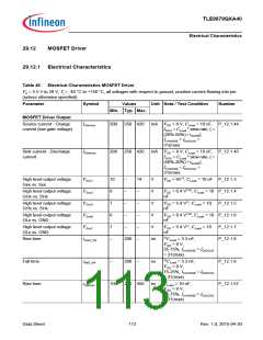
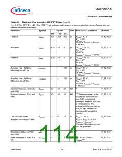
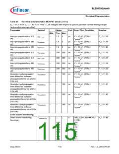
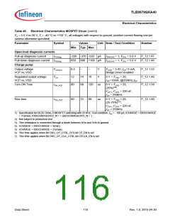
Table 41
Electrical Characteristics Operational Amplifier
VS = 5.5 V to 28 V, Tj = -40 °C to +150 °C; all voltages with respect to ground, positive current flowing into pin
(unless otherwise specified)
Parameter
Symbol
Values
Typ.
Unit Note / Test Condition
Number
Min.
Max.
Differential gain
(uncalibrated)
G
Gain settings GAIN<1:0>: P_13.1.6
9.5
19
38
57
10
20
40
60
10.5
21
42
00
01
10
11
63
Differential input operating VIX
voltage range OP2 - OP1
-1.5 / G –
1.5 / G
2.0
V
V
G is the Gain specified
below
P_13.1.1
Operating. common mode VCM
inputvoltage range (referred
to GND (OP2 - GND) or
(OP1 - GND)
-2.0
-7.0
–
–
Input common mode has P_13.1.2
to be checked in
evaluation if it fits the
required range
Max. input voltage range
(referred to GND (OP_2 -
GND) or (OP1 - GND)
VIX
7.0
V
Max. rating of operational P_13.1.3
amplifier inputs, where
measurement is not done
Single ended output voltage VOUT
range (linear range)
VZERO
- 1.5
–
–
VZERO
+ 1.5
V
1)2) Offset output voltage 2 P_13.1.4
V ± 1.5V
Linearity error
Linearity error
Gain drift
EPWM
-15
15
1.0
1
mV
Maximum deviation from P_13.1.5
best fit straight line
divided by max. value of
differential output voltage
range (0.5V - 3.5V); this
parameter is determined
at G = 10.
EPWM_% -1.0
–
–
%
%
Maximum deviation from P_13.1.24
best fit straight line
divided by max. value of
differential output voltage
range (0.5V - 3.5V); this
parameter is determined
at G = 10.
-1
Gain drift after calibration P_13.1.7
at G = 10.
Data Sheet
117
Rev. 1.0, 2015-04-30

 INFINEON [ Infineon ]