TLE9879QXA40
Electrical Characteristics
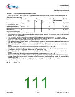
29.9.2
Electrical Characteristics ADC1 (10-Bit)
These parameters describe the conditions for optimum ADC performance.
Note:Operating Conditions apply.
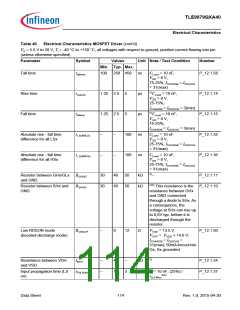
Table 38
A/D Converter Characteristics
VS = 5.5 V to 28 V, Tj = -40 °C to +150 °C; all voltages with respect to ground, positive current flowing into pin
(unless otherwise specified)
Parameter
Symbol
Values
Typ.
Unit
Note /
Test Condition
Number
Min.
Max.
1)
Analog reference supply VAREF
Analog reference ground VAGND
VAGND
+ 1.0
–
–
–
–
VDDPA
+ 0.05
V
P_9.2.1
P_9.2.2
P_9.2.3
VSS
- 0.05
1.5
V
–
2)
Analog input voltage
range
VAIN
VAGND
VAREF
24
V
3)
4)
Analog clock frequency fADCI
5
MHz
P_9.2.4
P_9.2.5
Conversion time for 10- tC10
bit result
(13 + STC) (13 + STC (13 + STC –
× tADCI ) × tADCI ) × tADCI
+ 2 x tSYS + 2 x tSYS + 2 x tSYS
Conversion time for 8-bit tC8
result
(11 + STC) (11 + STC (11 + STC –
–
P_9.2.6
P_9.2.7
P_9.2.8
× tADCI
) × tADCI
) × tADCI
+ 2 × tSYS + 2 × tSYS + 2 × tSYS
1)
Wakeup time from
analog powerdown, fast
mode
tWAF
–
–
–
–
4
µs
µs
5)
Wakeup time from
analog powerdown, slow
mode
tWAS
15
Total unadjusted error (8 TUE8B
bit)
–
–
±1
±6
±2
counts 6)7)VAREF = 5.0 V P_9.2.9
counts 7)8)VAREF = 5.0 V P_9.2.22
Total unadjusted error
(10 bit)
TUE10B
±12
DNL error
EADNL
–
–
±0.8
±0.8
±3
±5
counts –
counts –
P_9.2.10
P_9.2.11
INL error with internal 5V EAINL_int_V
reference VAREF
AREF
Gain error with internal
5V reference VAREF
EAGAIN_int_
–
±0.4
±10
counts –
counts –
P_9.2.12
VAREF
Offset error
EAOFF
–
–
±0.5
–
±2
10
P_9.2.13
P_9.2.14
5)9)
Total capacitance
of an analog input
CAINT
CAINS
RAIN
pF
pF
kΩ
5)9)
5)9)
Switched capacitance
of an analog input
–
–
–
–
4
2
P_9.2.15
P_9.2.16
Resistance of
the analog input path
Data Sheet
110
Rev. 1.0, 2015-04-30

 INFINEON [ Infineon ]