TLE9879QXA40
Electrical Characteristics
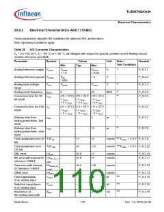
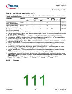
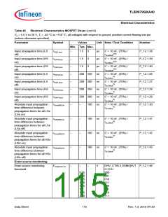
Table 38
A/D Converter Characteristics (cont’d)
VS = 5.5 V to 28 V, Tj = -40 °C to +150 °C; all voltages with respect to ground, positive current flowing into pin
(unless otherwise specified)
Parameter
Symbol
Values
Typ.
Unit
Note /
Test Condition
Number
Min.
Max.
5)9)
5)9)
5)9)
Total capacitance
of the reference input
CAREFT
CAREFS
RAREF
–
–
–
–
15
pF
pF
kΩ
P_9.2.17
P_9.2.18
P_9.2.19
Switched capacitance
of the reference input
–
–
7
2
Resistance of
the reference input path
1) Not subject to production test, specified by design.
2) VAIN may exceed VAGND or VAREFx up to the absolute maximum ratings. However, the conversion result in these cases will
be 0000H or 03FFH, respectively.
3) The limit values for fADCI must not be exceeded when selecting the peripheral frequency and the prescaler setting.
4) This parameter includes the sample time (also the additional sample time specified by STC), the time to determine the
digital result and the time to load the result register with the conversion result.
5) The broken wire detection delay against VAGND is measured in numbers of consecutive precharge cycles at a conversion
rate of not more than 500 µs.
6) The total unadjusted error TUE is the maximum deviation from the ideal ADC transfer curve, not the sum of individual
errors.
All error specifications are based on measurement methods standardized by IEEE 1241.2000.
7) The specified TUE is valid only if the absolute sum of input overload currents (see IOV specification) does not exceed
10 mA, and if VAREF and VAGND remain stable during the measurement time.
8) The total unadjusted error TUE is the maximum deviation from the ideal ADC transfer curve, not the sum of individual
errors.
All error specifications are based on measurement methods standardized by IEEE 1241.2000.
9) These parameter values cover the complete operating range. Under relaxed operating conditions (temperature, supply
voltage) typical values can be used for calculation. At room temperature and nominal supply voltage the following typical
values can be used:
CAINTtyp = 12 pF, CAINStyp = 5 pF, RAINtyp = 1.0 kꢀ, CAREFTtyp = 15 pF, CAREFStyp = 10 pF, RAREFtyp = 1.0 kꢀ.
29.10
Reserved
Data Sheet
111
Rev. 1.0, 2015-04-30

 INFINEON [ Infineon ]