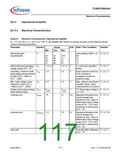
TLE9879QXA40
Electrical Characteristics
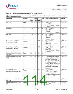
Table 41
Electrical Characteristics Operational Amplifier (cont’d)
VS = 5.5 V to 28 V, Tj = -40 °C to +150 °C; all voltages with respect to ground, positive current flowing into pin
(unless otherwise specified)
Parameter
Symbol
Values
Typ.
80
Unit Note / Test Condition
Number
Min.
Max.
DC input voltage common
mode rejection ratio
DC-
CMRR
58
–
dB
ns
CMRR (in dB)=-20*log
(differential mode gain/
common mode gain)
P_13.1.8
V
V
CMI= -2V... 2V,
AIP-VAIN=0V
Settling time to 98%
TSET
–
1
800
1400
1.5
Derived from 80 - 20 %
rise fall times for ± 2V
overload condition (3 Tau
value of settling time
constant)2)
P_13.1.9
2)
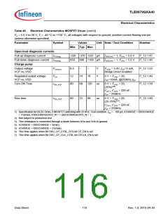
Current Sense Amplifier
Input Resistance @ OP1,
OP2
Rin_OP1_
1.25
kꢀ
–
P_13.1.25
OP2
1) Typical VZERO = 0,4 * VAREF.
2) This parameter is not subject to production test.
Data Sheet
118
Rev. 1.0, 2015-04-30

 INFINEON [ Infineon ]