TLE9879QXA40
Electrical Characteristics
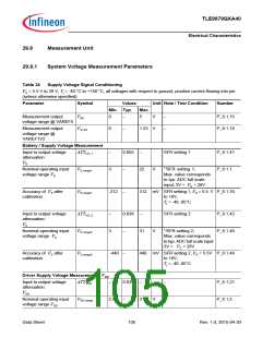
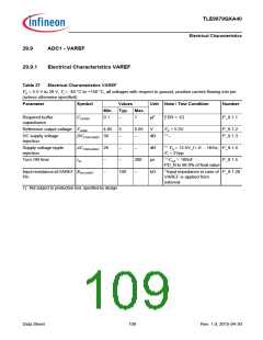
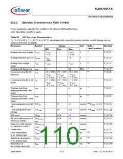
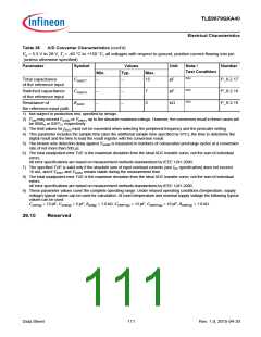
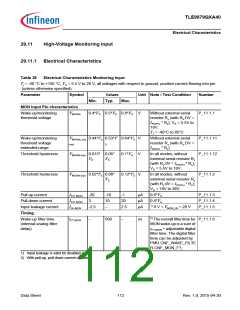
29.9
ADC1 - VAREF
29.9.1
Electrical Characteristics VAREF
Table 37
Electrical Characteristics VAREF
VS = 5.5 V to 28 V, Tj = -40 °C to +150 °C, all voltages with respect to ground, positive current flowing into pin
(unless otherwise specified)
Parameter
Symbol
Values
Unit Note / Test Condition
Number
Min. Typ. Max.
Required buffer
capacitance
CVAREF
0.1
–
1
µF
ESR < 1Ω
VS > 5.5V
P_9.1.1
Reference output voltage VAREF
4.95
5
–
5.05
–
V
P_9.1.2
P_9.1.3
1)
DC supply voltage
rejection
DCPSRVAREF 30
dB
–
1)
Supply voltage ripple
rejection
ACPSRVAREF 26
–
–
dB
µs
VS = 13.5V; f = 0 ... 1KHz; P_9.1.4
Vr = 2Vpp
Turn ON time
tso
–
–
–
200
–
1) Cext = 100nF
PD_N to 99.9% of final value
1)input impedance in case of P_9.1.20
VAREF is applied from
external
P_9.1.5
Input resistance at VAREF RIN,VAREF
Pin
100
kΩ
1) Not subject to production test, specified by design.
Data Sheet
109
Rev. 1.0, 2015-04-30

 INFINEON [ Infineon ]