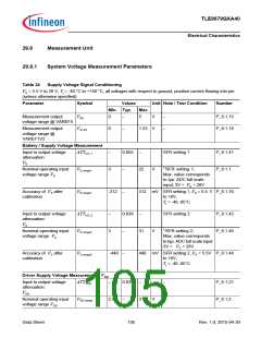
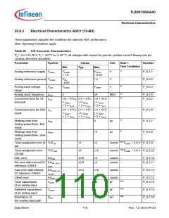
TLE9879QXA40
Electrical Characteristics
Table 34
Supply Voltage Signal Conditioning (cont’d)
VS = 5.5 V to 28 V, Tj = -40 °C to +150 °C, all voltages with respect to ground, positive current flowing into pin
(unless otherwise specified)
Parameter
Symbol
Values
Min. Typ.
-440 –
Unit Note / Test Condition
Number
Max.
Accuracy of VSD sense
after calibration
∆VSD
440 mV VS = 5.5V to 18V,
Tj = -40..85°C
P_8.1.47
Charge Pump Voltage Measurement VCP
Input to output voltage
attenuation:
VCP
ATTVCP
–
0.023
–
–
P_8.1.56
1)
Nominal operating input
VCP,range
2.5
–
52
V
P_8.1.7
voltage range VCP
Accuracy of VCP sense
after calibration
∆VCP
-747 –
747 mV VS = 5.5V to 18V,
Tj = -40..85°C
P_8.1.62
Monitoring Input Voltage Measurement VMON
Input to output voltage
attenuation:
ATTVMON
–
0.039
–
–
P_8.1.49
VMON
1)
Nominal operating input
voltage range VMON
VMON,range
2.5
–
–
31
V
P_8.1.8
Accuracy of VMON sense
after calibration
∆VMON
-440
440 mV VS = 5.5V to 18V,
Tj = -40..85°C
P_8.1.68
Pad Supply Voltage Measurement VVDDP
Input-to-output voltage
attenuation:
ATTVDDP
–
0.164
–
–
P_8.1.33
VDDP
1)
Nominal operating input
voltage range VDDP
VDDP,range
0
–
–
7.50
V
P_8.1.50
P_8.1.5
Accuracy of VDDP sense
after calibration
∆VDDP_SENSE
-105
105 mV 2)VS = 5.5 to 18V,
Tj = -40..85°C
10-Bit ADC Reference Voltage Measurement VAREF
Input to output voltage
attenuation:
ATTVAREF
–
0.219
–
–
P_8.1.22
VAREF
1)
Nominal operating input
voltage range VAREF
VAREF,range
0
–
–
5.62
79
V
P_8.1.51
P_8.1.48
Accuracy of VAREF sense ∆VAREF
after calibration
-79
mV VS = 5.5V to 18V,
Tj = -40..85°C
8-Bit ADC Reference Voltage Measurement VBG
Input-to-output voltage
attenuation:
VBG
ATTVBG
–
0.75
–
–
P_8.1.57
Data Sheet
106
Rev. 1.0, 2015-04-30

 INFINEON [ Infineon ]