TLE9879QXA40
Electrical Characteristics
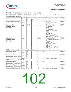
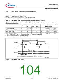
Table 32
Electrical Characteristics LIN Transceiver (cont’d)
Vs = 5.5V to 18V, Tj = -40 °C to +150 °C, all voltages with respect to ground, positive current flowing into pin
(unless otherwise specified)
Parameter
Symbol
Values
Typ.
Unit Note / Test Condition Number
Min.
Max.
Duty cycle D7 (for worst
case at 115 kbit/s)
for +1 µs Receiver delay
symmetry
tduty1
0.399
–
–
5) duty cycle D7
THRec(max) =
0.744 ×VS;
P_6.1.34
THDom(max) =
0.581 ×VS; VS = 13.5 V;
tbit = 8.7 µs;
D7 = tbus_rec(min)/2 tbit;
Duty cycle D8 (for worst
case at 115 kbit/s)
for +1 µs Receiver delay
symmetry
tduty2
–
–
0.578
5) duty cycle 8
THRec(min) = 0.422 ×VS;
THDom(min) =
0.284 ×VS;VS = 13.5 V;
tbit = 8.7 µs;
P_6.1.35
D8 = tbus_rec(max)/2 tbit;
6)
LIN input capacity
CLIN_IN
ttimeout
–
6
15
12
30
20
pF
P_6.1.69
P_6.1.36
TxD dominant time out
ms
V
TxD = 0 V
Thermal Shutdown (Junction Temperature)
6)
6)
Thermal shutdown temp.
Thermal shutdown hyst.
TjSD
160
–
180
10
200
–
°C
K
P_6.1.65
P_6.1.66
∆T
1) Maximum limit specified by design.
2) VBUS_CNT = (Vth_dom +Vth rec)/2
3) VHYS = VBUSrec - VBUSdom
4) Bus load concerning LIN Spec 2.2:
Load 1 = 1 nF / 1 kΩ = CBUS / RBUS
Load 2 = 6.8 nF / 660 Ω = CBUS / RBUS
Load 3 = 10 nF / 500 Ω = CBUS / RBUS
5) Bus load
Load 1 = 1 nF / 500 Ω = CBUS / RBUS
6) Not subject to production test, specified by design.
Data Sheet
103
Rev. 1.0, 2015-04-30

 INFINEON [ Infineon ]