TLE9879QXA40
Electrical Characteristics
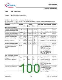
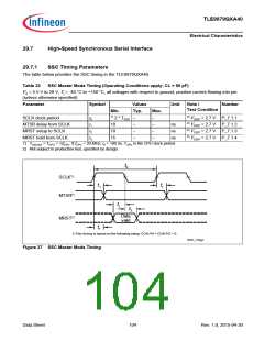
29.7
High-Speed Synchronous Serial Interface
SSC Timing Parameters
29.7.1
The table below provides the SSC timing in the TLE9879QXA40.
Table 33 SSC Master Mode Timing (Operating Conditions apply; CL = 50 pF)
VS = 5.5 V to 28 V, Tj = -40 °C to +150 °C, all voltages with respect to ground, positive current flowing into pin
(unless otherwise specified)
Parameter
Symbol
Values
Unit
Note /
Number
Test Condition
Min.
Typ.
Max.
SCLK clock period
t0
t1
t2
t3
1) 2 * TSSC
–
–
–
–
–
–
–
–
2) VDDP > 2.7 V P_7.1.1
2) VDDP > 2.7 V P_7.1.2
2) VDDP > 2.7 V P_7.1.3
2) VDDP > 2.7 V P_7.1.4
MTSR delay from SCLK
MRST setup to SCLK
MRST hold from SCLK
10
10
15
ns
ns
ns
1) TSSCmin = TCPU = 1/fCPU. If fCPU = 20 MHz, t0 = 100 ns. TCPU is the CPU clock period.
2) Not subject to production test, specified by design.
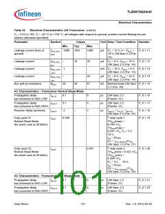
t0
SCLK1)
t1
t1
1)
MTSR
t2
t3
Data
valid
MRST1)
t1
1) This timing is based on the following setup: CON.PH = CON.PO = 0.
SSC_Tmg1
Figure 37 SSC Master Mode Timing
Data Sheet
104
Rev. 1.0, 2015-04-30

 INFINEON [ Infineon ]