TLE9879QXA40
Electrical Characteristics
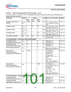
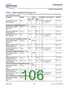
Table 32
Electrical Characteristics LIN Transceiver (cont’d)
Vs = 5.5V to 18V, Tj = -40 °C to +150 °C, all voltages with respect to ground, positive current flowing into pin
(unless otherwise specified)
Parameter
Symbol
Values
Typ.
Unit Note / Test Condition Number
Min.
Max.
Receiver delay symmetry
tsym,R
tduty1
-2
–
2
µs
t
sym,R = td(L),R - td(H),R
;
P_6.1.23
P_6.1.24
LIN Spec 2.2 (Par. 32)
Duty cycle D3
(for worst case at
10,4 kbit/s)
0.417
–
–
4) duty cycle 3
THRec(max) =
0.778 ×VS;
THDom(max) =
0.616 ×VS; VS = 5.5 …
18 V;
tbit = 96 µs;
D3 = tbus_rec(min)/2 tbit;
LIN Spec 2.2 (Par. 29)
Duty cycle D4
(for worst case at
10,4 kbit/s)
tduty2
–
–
0.590
4) duty cycle 4
THRec(min) = 0.389 ×VS;
THDom(min) =
P_6.1.25
0.251 ×VS;
VS = 5.5 … 18 V;
tbit = 96 µs;
D4 = tbus_rec(max)/2 tbit;
LIN Spec 2.2 (Par. 30)
AC Characteristics - Transceiver Fast Slope Mode
Propagation delay
bus dominant to RxD LOW
td(L),R
td(H),R
tsym,R
0.1
0.1
-1.5
–
–
–
6
µs
µs
µs
–
–
P_6.1.26
P_6.1.27
P_6.1.28
Propagation delay
bus recessive to RxD HIGH
6
Receiver delay symmetry
1.5
t
sym,R = td(L),R - td(H),R
;
AC Characteristics - Flash Mode
Propagation delay
bus dominant to RxD LOW
td(L),R
td(H),R
tsym,R
0.1
0.1
-1.0
–
–
–
6
µs
µs
µs
–
–
P_6.1.31
P_6.1.32
P_6.1.33
Propagation delay
bus recessive to RxD HIGH
6
Receiver delay symmetry
1.5
tsym,R = td(L),R - td(H),R
;
Data Sheet
102
Rev. 1.0, 2015-04-30

 INFINEON [ Infineon ]