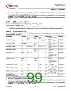
TLE9879QXA40
Electrical Characteristics
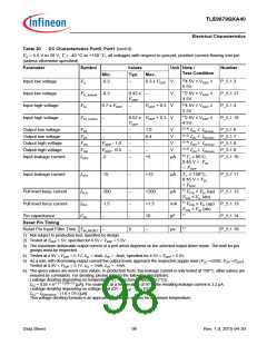
Table 30
DC Characteristics Port0, Port1 (cont’d)
VS = 5.5 V to 28 V, Tj = -40 °C to +150 °C, all voltages with respect to ground, positive current flowing into pin
(unless otherwise specified)
Parameter
Symbol
Values
Typ.
–
Unit Note /
Test Condition
Number
Min.
Max.
Input low voltage
Input low voltage
Input high voltage
Input high voltage
VIL
-0.3
0.3 x VDDP
V
2)4.5V ≤ VDDP
≤
≤
≤
≤
P_5.1.3
P_5.1.17
P_5.1.4
P_5.1.18
5.5V
VIL_extend -0.3
0.42 x
VDDP
–
V
1)2.6V ≤ VDDP
4.5V
VIH
0.7 x VDDP
–
V
DDP + 0.3 V
2)4.5V ≤ VDDP
5.5V
VIH_extend
–
0.52 x VDDP + 0.3 V
1)2.6V ≤ VDDP
VDDP
4.5V
Output low voltage
Output low voltage
Output high voltage
Output high voltage
Input leakage current
VOL
VOL
VOH
VOH
IOZ2
–
–
–
–
–
–
1.0
0.4
–
V
V
V
V
3) 4) IOL ≤ IOLmax P_5.1.6
3) 5) IOL ≤ IOLnom P_5.1.7
3) 4) IOH ≥ IOHmax P_5.1.8
3) 5) IOH ≥ IOHnom P_5.1.9
–
V
V
DDP - 1.0
DDP - 0.4
–
-5
+5
µA 6) TJ ≤ 85°C,
0.45 V < VIN
< VDDP
P_5.1.10
Input leakage current
IOZ2
-15
–
+15
µA TJ ≤ 150°C,
0.45 V < VIN
< VDDP
P_5.1.11
Pull level keep current
Pull level force current
IPLK
IPLF
CIO
-200
-1.5
–
–
–
–
+200
+1.5
10
µA 7) VPIN ≥ VIH (up) P_5.1.12
PIN ≤ VIL (dn)
mA 7) VPIN ≤ VIL (up) P_5.1.13
V
VPIN ≥ VIH (dn)
1)
Pin capacitance
pF
µs
P_5.1.14
P_5.1.19
Reset Pin Timing
1)
Reset Pin Input Filter Time Tfilt_RESET
–
5
–
1) Not subject to production test, specified by design.
2) Tested at VDDP = 5V, specified for 4.5V < VDDP < 5.5V.
3) The maximum deliverable output current of a port driver depends on the selected output driver mode. The limit for pin
groups must be respected.
4) Tested at 4.9V < VDDP < 5.1V, IOL = 4mA, IOH = -4mA, specified for 4.5V < VDDP < 5.5V.
5) As a rule, with decreasing output current the output levels approach the respective supply level (VOL→GND, VOH→VDDP).
Tested at 4.9V < VDDP < 5.1V, IOL = 1mA, IOH = -1mA.
6) The given values are worst-case values. In production tests, this leakage current is only tested at 150°C; other values are
ensured by correlation. For derating, please refer to the following descriptions:
Leakage derating depending on temperature (TJ = junction temperature [°C]):
I
OZ = 0.05 × e(1.5 + 0.028×TJ) [µA]. For example, at a temperature of 95°C the resulting leakage current is 3.2 µA.
Leakage derating depending on voltage level (DV = VDDP - VPIN [V]):
OZ = IOZtempmax - (1.6 × DV) [µA]
This voltage derating formula is an approximation which applies for maximum temperature.
I
Data Sheet
98
Rev. 1.0, 2015-04-30

 INFINEON [ Infineon ]