OPTIREG™ SBC TLE9274QXV33
Fail-safe outputs and fail-safe input
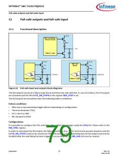
Note: The fail outputs are triggered for any of the above described failures and not only for failures leading to
the Fail-Safe mode.
The three fail outputs are activated in parallel. The FO1 gives a static LOW signal in case of fail output
activation. The FO2 provides a signal with a fixed frequency pulse and a duty cycle of 50% to generate an
indicator signal. The FO3 provides a PWM signal with a fixed frequency and duty cycle of 20%, e.g. to generate
a dimmed bulb signal.
Fail outputs
•
•
•
FO1: Static fail output
FO2: 1.25 Hz 50% duty cycle (typ.)
FO3: 100 Hz 20% duty cycle (typ.)
Pull-up configuration
The integrated pull-up resistors are active if following conditions are fulfilled:
•
•
•
FO1: SBC Init mode OR SBC Normal mode
FO2: (SBC Init mode OR SBC Normal mode) AND FSI_FO2 = 0
FO3: SBC Init mode
12.2
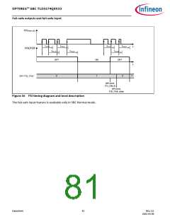
Fail-safe input
The FO2 pin can be used as safety feature called fail-safe input.
A digital signal has to be generated by the microcontroller and the TLE9274QXV33 must detect the Low-to-
High transition whitin tFSI,W window time. The feature is enabled by default after power on. It can be disabled
using the SPI command (FSI_FO2=1 on HW_CTRL register).
If there is no signal from the microcontroller, the TLE9274QXV33 sets the FSI_FAIL on DEV_STAT and both FO1
and FO3 are activated. The device remains in the same mode and neither reset nor interrupt will be triggered.
The SPI status bit FSI_FAIL can only be cleared after a new rising edge on the FSI pin.
The Figure 36 shows the timing diagram and level description of FSI input signal.
Datasheet
80
Rev.2.0
2022-05-06

 INFINEON [ Infineon ]