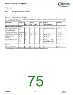
OPTIREG™ SBC TLE9274QXV33
Fail-safe outputs and fail-safe input
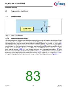
12
Fail-safe outputs and fail-safe input
12.1
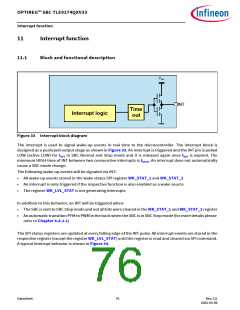
Functional description
5V_int
SBC Init Mode /
Normal mode
RFO1
FO1
Failure Logic
5V_int
5V_int
SBC Init
Mode
T FSI
RFSI
T test
RTEST
FO2/FSI
FO3/TEST
T FO_PL
T FO_PL
Failure Logic
Failure Logic
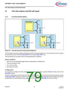
Figure 35 Fail-safe input and outputs block diagrams
The fail outputs consist of a failure logic block and three low-side switches. In case of a failure, the FO outputs
are activated and the SPI bit FO_ON_STATE in the register DEV_STAT is set.
The fail outputs are activated under the following failure conditions:
Failure conditions
•
•
•
•
After one or two watchdog trigger failures depending on configuration
Thermal shutdown TSD2
VCC1 short to GND
RO clamped to HIGH
Configurations
It is possible to configure the FOx activation after a Watchdog trigger using the CFG2 bit. Please refer to the
HW_CTRL register.
In order to deactivate the fail output, the failure conditions (e.g. TSD2) must not be present anymore and the
bit FO_ON_STATE needs to be cleared via SPI command. In case of watchdog fail, the fail output may only be
disabled after the watchdog has been triggered successfully, i.e. the WD_FAIL bit must be cleared.
Datasheet
79
Rev.2.0
2022-05-06

 INFINEON [ Infineon ]