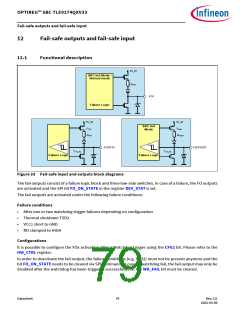
OPTIREG™ SBC TLE9274QXV33
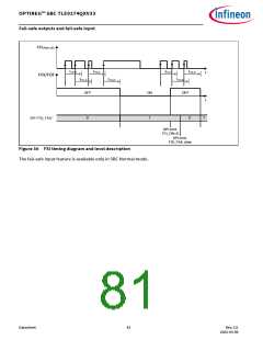
Fail-safe outputs and fail-safe input
12.3
Electrical characteristics
Table 19 Interrupt output
Tj = -40°C to +150°C; VS = 5.5 V to 28 V; SBC Normal mode; all voltages with respect to ground; positive current
defined flowing into pin (unless otherwise specified)
Parameter
Symbol
Values
Typ.
Unit Note or
Test Condition
Number
Min.
Max.
Fail output; pin FO1, FO2, FO3
FO LOW output voltage
(active)
VFO,L
IFO,H
–
0
0.6
–
1
2
V
IFO = 5 mA
P_12.3.1
P_12.3.2
FO HIGH output current
(inactive)
µA
VFO = 28 V
FO3 test mode select
FO3/TEST HIGH-input
voltage threshold
VTEST,H
VTEST,L
–
–
–
0.7 ×
VCC1
V
–
P_12.3.28
P_12.3.29
P_12.3.30
P_12.3.31
P_12.3.32
FO3/TEST LOW-input
voltage threshold
0.3 ×
VCC1
–
–
–
–
V
–
1)
FO3/Hysteresis of TEST
input voltage
VTEST,Hys
–
–
–
0.2 ×
VCC1
V
FO3/Pull-up resistance at RTEST
pin TEST
5
kΩ
µs
VTEST = 0.2 × VCC1
1)
FO3/TEST input filter time tTEST
16
FO2/FSI input select
FSI HIGH-input voltage
threshold
VFSI,H
VFSI,L
–
–
–
0.7 ×
VCC1
V
V
V
–
P_12.3.6
P_12.3.7
P_12.3.8
FSI LOW-input voltage
threshold
0.3 ×
VCC1
–
–
1)
FSI hysteresis of input
voltage
VFSI,Hys
–
0.2 ×
VCC1
–
FSI pull-up resistance
FSI input filter time
FSI window time
FO1
RFSI
tFSI
–
–
–
40
–
–
kΩ
µs
µs
VFSI = 0.2 × VCC1
P_12.3.9
P_12.3.10
P_12.3.11
1)
1.5
240
1)
tFSI,W
–
1)
FO1 pull-up resistance
RFO1
–
40
–
kΩ
V
= 0.2 × VCC1
P_12.3.12
FO1
1) Not subject to production test; specified by design.
Datasheet
82
Rev.2.0
2022-05-06

 INFINEON [ Infineon ]