OPTIREG™ SBC TLE9274QXV33
Application information
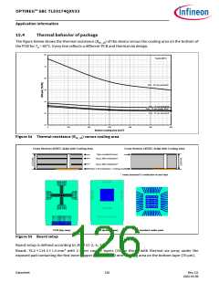
15.4
Thermal behavior of package
The figure below shows the thermal resistance (Rth_JA) of the device versus the cooling area on the bottom of
the PCB for TA = 85°C. Every line reflects a different PCB and thermal via design.
80
Tamb=85°C
70
60
2s0p - 25 vias (standard)
50
40
2s2p - 16 vias (standard)
2s2p - 16 vias (solder filled)
30
20
2s2p - 25 vias (standard)
0
100
200
300
400
500
600
Bottom Cooling area (mm2)
Figure 54 Thermal resistance (Rth_JA) versus cooling area
Cross Section (JEDEC 2s2p) with Cooling Area
Cross Section (JEDEC 2s0p) with Cooling Area
70µm modelled (traces)
35µm, 90% metalization*
35µm, 90% metalization*
70µm / 5% metalization + cooling area
*: means percentual Cu metalization on each layer
PCB (top view)
PCB (bottom view)
standard solder pads
Figure 55 Board setup
Board setup is defined according to JESD 51-2,-5,-7.
Board: 76.2 × 114.3 × 1.5 mm3 with 2 inner copper layers (35 µm thick), with thermal via array under the
exposed pad contacting the first inner copper layer and 300 mm2 cooling area on the bottom layer (70 µm).
Datasheet
126
Rev.2.0
2022-05-06

 INFINEON [ Infineon ]