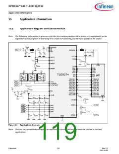
OPTIREG™ SBC TLE9274QXV33
Serial Peripheral Interface
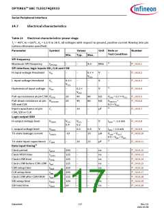
Table 23 Electrical characteristics: power stage (cont’d)
Tj = -40°C to +150°C, VS = 5.5 V to 28 V, all voltages with respect to ground, positive current flowing into pin
(unless otherwise specified)
Parameter
Symbol
Values
Typ.
–
Unit Note or
Test Condition
Number
Min.
Max.
Input signal rise time at pin trIN
SDI, CLK and CSN
–
50
ns
ns
µs
µs
–
P_14.8.21
P_14.8.22
P_14.8.23
P_14.8.24
Input signal fall time at pin tfIN
SDI, CLK and CSN
–
–
3
–
–
–
50
10
–
–
–
–
Delay time for mode
changes2)
tDel,Mode
CSN HIGH time
Data output timing1)
SDO rise time
tCSN(high)
trSDO
–
–
–
–
–
30
30
–
80
80
50
50
50
ns
ns
ns
ns
ns
CL = 100 pF
CL = 100 pF
P_14.8.25
P_14.8.26
SDO fall time
tfSDO
SDO enable time
SDO disable time
SDO valid time
tENSDO
tDISSDO
tVASDO
LOW impedance P_14.8.27
HIGH impedance P_14.8.28
–
–
CL = 100 pF
P_14.8.29
1) Not subject to production test; specified by design.
2) Applies to all mode changes triggered via SPI commands.
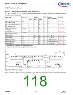
24
CSN
15
16
17
18
13
14
CLK
SDI
19
20
LSB
MSB
MSB
not defined
27
28
29
SDO
Flag
LSB
Figure 50 SPI timing diagram
Note: Numbers in drawing correlate to the last 2 digits of the number field in the electrical characteristics table.
Datasheet
118
Rev.2.0
2022-05-06

 INFINEON [ Infineon ]