TLE9263QX
System Features
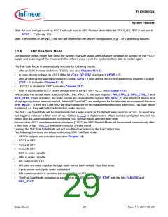
Note:An over voltage event on VCC1 will only lead to SBC Restart Mode if the bit VCC1_OV_RST is set and if
CFGP = ‘1’ (Config 1/3).
Note:The content of the WD_FAIL bits will depend on the device configuration, e.g. 1 or 2 watchdog failures.
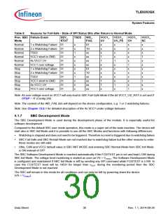
5.1.6
SBC Fail-Safe Mode
The purpose of this mode is to bring the system in a safe status after a failure condition by turning off the VCC1
supply and powering off the microcontroller. After a wake event the system is then able to restart again.
The Fail-Safe Mode is automatically reached for following events:
•
•
•
after an SBC thermal shutdown (TSD2) (see also Chapter 15.9.3),
in case of over voltage on VCC1 if the bit VCC1_OV_RST is set and if CFGP = ‘0’,
after a 1st incorrect watchdog trigger in Config2 (CFG = 1) and after a 2nd incorrect watchdog trigger in Config4
(CFG = 0) (see also Chapter 5.1.1),
•
•
if VCC1 is shorted to GND (see also Chapter 15.7),
After 4 consecutive VCC1 under voltage events (only if VS > VS,UV, see Chapter 15.6).
In this case, the default wake sources (CAN, LINx, WK1...3, see also registers WK_CTRL_2, BUS_CTRL_1 and
BUS_CTRL_2) are activated, the wake events are cleared in the register WK_STAT_1, and all output drivers and
all voltage regulators are switched off. When WK1 and WK2 are configured for the alternate measurement function
(WK_MEAS = 1) then WK1 and WK2 will stay configured for the measurement function when SBC Fail-Safe Mode
is entered, i.e. they will not be activated as wake sources.
The SBC Fail-Safe Mode will be maintained until a wake event on the default wake sources occurs. To avoid any
fast toggling behavior a filter time of typ. 100ms (tFS,min) is implemented. Wake events during this time will be
stored and will automatically lead to entering SBC Restart Mode after the filter time.
In case of an VCC1 over temperature shutdown (TSD2) the SBC Restart Mode will be reached automatically after
a filter time of typ. 1s (tTSD2) without the need of a wake event.
Leaving the SBC Fail-Safe Mode will not result in deactivation of the Fail Output pins.
The following functions are influenced during SBC Fail-Safe Mode:
•
•
•
•
•
•
•
•
•
•
•
All FOx outputs are activated (see also Chapter 14)
VCC1 is OFF
VCC2 is OFF
VCC3 is OFF
CAN is wake capable
LINx is wake capable
HS Outputs are OFF
WK pins are wake capable through static sense (with default 16µs filter time)
Cyclic sense and Cyclic wake is disabled
SPI communication is disabled because VCC1 is OFF
The Fail-Safe Mode activation is signalled in the SPI register DEV_STAT with the bits FAILURE and
DEV_STAT
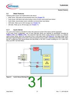
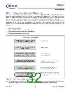
Data Sheet
29
Rev. 1.1, 2014-09-26

 INFINEON [ Infineon ]