TLE9263QX
System Features
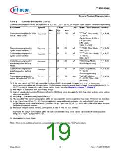
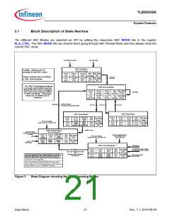
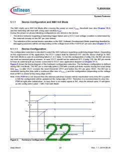
There are four different device configurations (Table 5) available defining the watchdog failure and the VCC1 over
voltage behavior. The configurations can be selected via the external connection on the INT pin and the SPI bit
CFG in the HW_CTRL register (see also Chapter 16.4):
•
CFGP = ‘1’: Config 1 and Config 3:
–
A watchdog trigger failure leads to SBC Restart Mode and depending on CFG the Fail Outputs (FOx) are
activated after the 1st (Config 1) or 2nd (Config 3) watchdog trigger failure;
–
A VCC1 over voltage detection will lead to SBC Restart Mode if VCC1_OV_RST is set.
VCC1_ OV will be set and the Fail Outputs are activated;
•
CFGP = ‘0’: Config 2 and Config 4:
–
A watchdog trigger failure leads to SBC Fail-Safe Mode and depending on CFG the Fail Outputs (FOx) are
activated after the 1st (Config 2) or 2nd (Config 4) watchdog trigger failure. The first watchdog trigger failure
in Config 4 will lead to SBC Restart Mode;
–
A VCC1 over voltage detection will lead to SBC Fail-Safe Mode if VCC1_OV_RST is set.
VCC1_ OV will be set and the Fail Outputs are activated;
The respective device configuration can be identified by reading the SPI bit CFG in the HW_CTRL register and
the CFGP bit in the WK_LVL_STAT register.
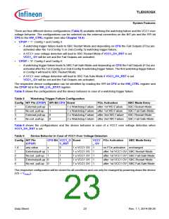
Table 5 shows the configurations and the device behavior in case of a watchdog trigger failure:
Table 5
Watchdog Trigger Failure Configuration
Config INT Pin (CFGP) SPI Bit CFG Event
FOx Activation
SBC Mode Entry
SBC Restart Mode
SBC Fail-Safe Mode
SBC Restart Mode
SBC Fail-Safe Mode
1
2
3
4
External pull-up
No ext. pull-up
External pull-up
No ext. pull-up
1
1
0
0
1 x Watchdog Failure after 1st WD Failure
1 x Watchdog Failure after 1st WD Failure
2 x Watchdog Failure after 2nd WD Failure
2 x Watchdog Failure after 2nd WD Failure
Table 6 shows the configurations and the device behavior in case of a VCC1 over voltage detection when
VCC1_OV_RST is set:
Table 6
Device Behavior in Case of VCC1 Over Voltage Detection
Config INT Pin
(CFGP)
CFG Bit VCC1_O Event
V_RST
VCC1 FOx Activation
_ OV
SBC Mode Entry
1-4
1
any value
Externalpull-up 1
No ext. pull-up
Externalpull-up 0
No ext. pull-up
x
0
1
1
1
1
1 x VCC1 OV
1 x VCC1 OV
1 x VCC1 OV
1 x VCC1 OV
1 x VCC1 OV
1
1
1
1
1
no FOx activation unchanged
after 1st VCC1 OV SBC Restart Mode
after 1st VCC1 OV SBC Fail-Safe Mode
after 1st VCC1 OV SBC Restart Mode
after 1st VCC1 OV SBC Fail-Safe Mode
2
1
3
4
0
The respective configuration will be stored for all conditions and can only be changed by powering down the device
(VS < VPOR,f).
Data Sheet
23
Rev. 1.1, 2014-09-26

 INFINEON [ Infineon ]